Morphology of an ITO recombination layer deposited on a silicon wire texture for potential silicon/perovskite tandem solar cell applications
Grazyna Kulesza-Matlak1
Marek Szindler2
Magdalena M. Szindler2
Anna Sypien1
Lukasz Major1
Kazimierz Drabczyk1
- Institute of Metallurgy and Materials Science, Polish Academy of Sciences, ul. W. Reymonta 25, 30-059 Kraków, Poland
- Faculty of Mechanical Engineering, Silesian University of Technology, ul. Akademicka 2A, 44-100 Gliwice, Poland
Article Info
Received 11 Jul. 2023
Received in revised form 17 Aug. 2023
Accepted 15 Sep. 2023
Available on-line 08 Nov. 2023
Keywords: Tandem solar cell; silicon nanowires; MAE etching; ITO; recombination layer.
Abstract
This paper presents research on the deposition of an indium tin oxide (ITO) layer which may act as a recombination layer in a silicon/perovskite tandem solar cell. ITO was deposited by magnetron sputtering on a highly porous surface of silicon etched by the metal-assisted etching method (MAE) for texturing as nano and microwires. The homogeneity of the ITO layer and the degree of coverage of the silicon wires were assessed using electron microscopy imaging techniques. The quality of the deposited layer was specified, and problems related to both the presence of a porous substrate and the deposition method were determined. The presence of a characteristic structure of the deposited ITO layer resembling a "match" in shape was demonstrated. Due to the specificity of the porous layer of silicon wires, the ITO layer should not exceed 80 nm. Additionally, to avoid differences in ITO thickness at the top and base of the silicon wire, the layer should be no thicker than 40 nm for the given deposition parameters.
Introduction
The two main factors limiting the efficiency of singlejunction solar cells are limited absorption of photons with energies below the bandgap and thermalization losses. Considering these factors, the natural consequence is the integration of materials, the so-called absorbers with different bandgaps in a multi-junction structure. The simplest method, which involves connecting a high-gap material on top of a low-gap material, is called a tandem structure [1]. In a tandem structure, a high-bandgap material is used as the upper sub-cell to effectively absorb high-energy (short wavelength) photons and transmit low-energy photons, i.e., lower than the bandgap of the absorber material that the solar cell is made of. The transmitted spectrum is directed to a material with a low bandgap (lower sub-cell) and is absorbed there. This process allows the collection of the maximum number of photons using a wide solar spectrum and minimizing the thermalization process [2].
For bottom absorbers, crystalline silicon (c-Si) solar cells are ideal candidates due to their cost-competitive manufacturing (based on their market dominance), highopen- circuit voltage down to 0.75 V, high efficiency, and the corresponding bandgap value (1.1 eV). Technology development so far has allowed the use of many different materials in the search for the best upper sub-cell to match the silicon solar cell. The breakthrough moment turned out to be the use of a material that is simple and cheap to obtain, showing high efficiency and excellent optoelectronic parameters – a material with a significant development potential, i.e., perovskite. High absorption of photons in the material, ability to control the bandgap over a wide spectrum range, high value of open-circuit voltage, and length of diffusion path made it possible to be perfectly paired with the silicon cell. Perovskites have attracted the attention of the scientific community with an unprecedented increase in the photovoltaic conversion efficiency of solar cells made from them. The current efficiency record for a silicon/perovskite tandem solar cell has already surpassed the long-unattainable mark of 30% and now stands at 33.2% [2–4].
In an integrated (monolithic) tandem solar cell, top and bottom sub-cells must be optically and electrically connected with an interconnection layer or a tunnelling junction [5]. The tunnelling junction with good perfor-mance should have the following characteristics: the ability for efficient carrier collection or migration, sufficient recombination rate for lower VOC loss, and good spectral distribution function for current matching [6]. Transparent conductive oxide (TCO) materials are considered promising candidates. Knowing the excellent conductive properties [7], many research centres indicate indium tin oxide (ITO) as a material suitable for use as a recombinant layer [8–10].
The authors deal with the subject of silicon wafer texturization in the form of nano and microwires [11, 12]. The surface texture for solar cells is designed to reduce the reflection of solar radiation from the front surface of the silicon wafer. Such a treatment affects the penetration of more photons into the material which is necessary for the photovoltaic (PV) effect. Thus, texturization changes the surface morphology from relatively smooth to rough. The conducted research is based on the metal-assisted etching method (MAE). Such a method depends on the type of metal used in the reaction and the solution that will etch the silicon selectively in the presence of this metal. This means that regardless of the type of silicon that will be etched, the final effect in the form of a characteristic surface structure is the same for mono and polycrystalline silicon. In this paper, the authors used silver as a catalyst.
The obtained wires structure plays a double role: 1) reduction of solar radiation reflection in the wavelength range of 300–1200 nm to an effective value below 5% and 2) scaffolding for the perovskite layer in silicon/perovskite tandem cells. In the subject of tandem solar cells, methods of depositing a perovskite absorber on a classically textured silicon surface, mainly in the form of pyramids, have already been described [13–16] even on the industrial-size Si solar cells [17].
The novelty is covering a high porosity textured silicon surface consisting of chemically etched silicon wires while providing a scaffold for the perovskite absorber and maintaining an excellent reflection reduction to improve the entire cell power. To the authors’ knowledge, this is the first proposal and attempt to implement etched silicon wires into the structure of a silicon/perovskite tandem cell. The first attempts to cover silicon wires with perovskite have already been published [12] but this article presents the results of research on covering silicon wires with an ITO recombination layer and an assessment of its homogeneity in terms of the applied deposition technique.
Tandem solar cells based on crystalline silicon and perovskite are beginning to be commercialized and show great potential to replace current silicon devices and lead the way in long-term PV technologies. Efforts of scientists and significant financial outlays give hope for the widespread presence of tandem modules in the perspective of the coming years [17–19].
Materials
The Czochralski monocrystalline p-type (100) silicon wafers were chosen for further examination. The first step was chemical polishing in a solution of 30% KOH (85% POCH pure p.a.) at an elevated temperature of 70 C. The etching time corresponded to a thickness of an etched layer of at least 15 μm per side. On such prepared wafers, the surface texture in the form of silicon wires was etched.
The wires were formed using the MAE process using silver as a catalyst. The first stage was the purification of a silicon wafer from intrinsic silicon dioxide in a 5 M HF solution (40% CHEMPUR pure p.a.). Then, the hydrophobic silicon surface was wetted with methyl alcohol (CHEMPUR pure p.a.). The silver nanoparticles deposition was proceeded by dipping in a 0.02 M aqueous solution of silver nitrate (> 99.8% Sigma-Aldrich pure p.a.) in DI water, acidified with 5 M HF in a volume ratio of 1:1 at a time of 20 s. The etching process was carried out in HF:H2O2 solution with a 10:1 volume ratio at a time of 10, 20, and 30 s leading to a homogeneous structure of wires of a specific height equal to average values of 234, 377, and 550 nm, respectively [12].
Results
Based on the research conducted on systematising the size and distribution of nano and microwires through the appropriate selection of chemical etching parameters, a compromise was made between the optical properties and the possibility of producing a solar cell. High wires, above 5 m, show high absorption due to the effective trapping of light in the spaces between them (multiple reflections), while the deposition of successive layers in a homogeneous manner on such a porous substrate becomes problematic [11]. This is difficult both in the case of a silicon solar cell (passivation, metallic electrodes) and a tandem solar cell (recombination layer, top-cell layer). Short wires may allow a subsequent uniform layer deposition but do not provide the maximum optical effect. An accepted compromise is the presence of wires with lengths in the range of 200–500 nm.
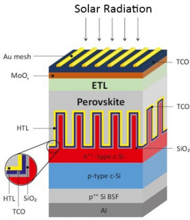
The research is focused on the tandem solar cell presented in Fig. 1. The possibility of deposition and the properties of the recombination layer were analysed choosing ITO as a reference material. The ITO layer in the tandem structure is directly on the surface of the wires as shown in Fig. 1 because the SiO2 layer is optional. In the diagram, the recombination layer is marked as TCO. It is important that the obtained layer should uniformly cover the wires and also the spaces between them.
The ITO layer was deposited by magnetron sputtering using a Plasmionique SPT320-PE reactor using the following parameters: power 60 W, voltage on the substrate 50 V, pressure in the chamber 10 mTorr. The first stage of the study was to examine the optical parameters of the ITO layers depending on their thickness. The tests were carried out using a Lambda 950S spectrophotometer by Perkin Elmer in the total trans-mission measurement mode with an integrating sphere in the wavelength range of 250–1200 nm.
The short-wave range in transmission studies is negligible due to the absorption of high-energy radiation by the perovskite solar cell. Fig. 2 shows the graph of the total transmission depending on a layer thickness as a function of wavelength for the ITO layer deposited on a microscope slide in the wavelength range of 500–1200 nm.

ITO layers show high transmission in the studied wavelength range which decreases with increasing thickness. The thickness of the layers was estimated using a reflectometer FR-pRo-UV/VIS (ThetaMetrisis SA, Peristeri Greece) in the reflection mode in the wavelength range of 300–800 nm. Estimated thickness values are shown in Table 1.
Table 1.
ITO layer thickness values estimated using a reflectometer.
ITO layer – deposition time |
Estimated thickness |
PVD_20 min |
40 nm |
PVD_40 min |
60 nm |
PVD_60 min |
80 nm |
The next study stage consisted of visually checking whether the applied ITO layer is homogeneous and whether it fills the spaces between the wires. The surface morphology was examined using the scanning electron microscopy (SEM) technique using a QUANTA 200 3D Dual Beam (FEI). For a detailed study of the microstructure, a transmission electron microscopy (TEM) technique was used with a Tecnai G2 F20 (200 kV) equipped with a field-emission gun (FEG) and a HAADF detector for observation with the scanning transmission electron microscopy (STEM) technique.
Firstly, SEM micrographs were taken. Three types of samples differing in sizes of wires were used for the tests, marked according to a proper etching time of 10, 20, and 30 s. ITO layers were applied on such prepared substrates with deposition time and estimated thickness indicated in Table 1. The SEM micrographs taken are shown in Figs. 3–5.


The deposited ITO layers reveal a tendency to form match-like structures. This means that in the upper part, the layer seems to be thicker and disappears towards bulk silicon. As the thickness of the ITO layer increases, the character of the "match" is more visible, creating, for the thickest layer, a spherical structure resembling a head. Wires without the ITO layer do not have such shape, and even narrow towards the top which results from etching into the silicon wafer. SEM studies were important from the point of view of the general characteristics of the applied ITO layers and showed that the layer is not completely homogeneous. However, they did not answer whether the layer completely covered the wires and whether it was deposited in the deepest spaces between the wires, namely at the base of the wires. Therefore, thin films, so-called lamellas for TEM observations, were prepared by the focused ion beam (FIB) technique, and TEM imaging was performed along with an energy dispersive spectroscopy (EDS) microanalysis of the chemical compo-sition. A sample with the thinnest ITO layer (shortest deposition time) was selected for the tests to check the presence of a layer fully covering the wires. The results are shown in Fig. 6.

STEM micrographs revealed that the ITO layer completely covers the wires, but not uniformly. Enrichment in indium, tin, and oxygen is visible in the upper part of the wires, but the presence of an ITO layer in the lower part of the wires has also been confirmed. The shape of the wires themselves was also confirmed, which, narrowing towards the top, resemble the shape of a "needle". This means that the "match" observed in the SEM and STEM micrographs is the result of non-homogeneity in the deposition of the ITO layer.
Conclusions
On the porous silicon surface, consisting of chemically etched wires, an ITO layer was deposited by magnetron sputtering which acts as a recombination layer in a silicon/perovskite tandem solar cell. Depending on the thickness of the ITO layer, its optical properties were examined which are characterised by a high transmission in the wavelength range above 500 nm, i.e., for radiation that should be effectively transmitted to the bottom cell, in this case, silicon.
Examination of the silicon microstructure with wires and sputtered ITO layer showed that the applied layer completely covers the wires in the spaces between the wires, but forms the shape of a "match" which means that it is thicker in the upper part of the wire. This effect increases as the ITO layer thickens.
The detailed value of the ITO thickness in porous scaffold is not obvious. Information on the optimal thickness of the ITO-based recombination layer is available in the literature, these are both calculated and empirically measured values. Unfortunately, they refer to a flat sample. In the case of a sample with a scaffold based on silicon nanowires, the optimal value must be a compromise between the conductivity of the layer, transmittance, and filling the space between the wires. Since the work concerns research on materials engineering, it should be stated that considering the spaces between the wires, the ITO layer should not be thicker than 80 nm. If the optical and electrical parameters are not sufficient, the application technique (stoichiometry control) or the type of layer should be changed.
In this particular case, using the given embedding parameters, the magnetron sputtering method can be used for small thicknesses of ITO layers (up to 40 nm), whereas when it is necessary to use thicker layers, other methods of layer deposition should be used.
Authors’ statement
Authors contributions: research concept and design: G.K.-M., M.S., M.M.S.; collection and/or assembly of data: G.K.-M., M.S., M.M.S., A.S., L.M.; data analysis and interpretation: G.K.-M., A.S., L.M., K.D.; writing the article: G.K.-M.; critical revision of the article: M.S., M.M.S., K.D.; final approval of article: G.K.-M., M.S., M.M.S., A.S., L.M., K.D.
Acknowledgements
This research was funded by IMMS PAS as a statutory work. The transmission measurements, as well as SEM and TEM examinations, were performed in the Accredited Testing Laboratories at the IMMS PAS (ILAC-MRA).
References
-
Hu, Y., Song, L., Chen, Y. & Huang, W. Two-terminal perovskites tandem solar cells: recent advances and perspectives. Sol. RRL 3, 1900080 (2019). https://doi.org/10.1002/solr.201900080
-
Jošt, M., Kegelmann, L., Korte, L. & Albrecht, S. Monolithic perovskite tandem solar cells: a review of the present status and advanced characterization methods toward 30% efficiency. Adv. Energy Mater. 10, 1904102 (2020). https://doi.org/10.1002/aenm.201904102
-
Li, X. et al. Silicon heterojunction-based tandem solar cells: past, status, and future prospects. Nanophotonics 10, 2001–2022 (2021). https://doi.org/10.1515/nanoph-2021-0034
-
Best Research-Cell Efficiency Chart. Photovoltaic Research(accesed: April, 15th, 2023) https://www.nrel.gov/pv/cell-efficiency.html
-
Li, C., Wang, Y. & Choy, W. C. H. Efficient interconnection in perovskite tandem solar cells. Small Methods 4, 2000093 (2020). https://doi.org/10.1002/smtd.202000093
-
Chen, B. et al. Insights into the development of monolithic perovskite/silicon tandem solar cells. Adv. Energy Mater. 12, 2003628 (2021). https://doi.org/10.1002/smtd.202003628
-
Drabczyk, K., Kulesza-Matlak, G., Drygała, A., Szindler, M. & Lipiński, M. Electroluminescence imaging for determining the influence of metallization parameters for solar cell metal contacts. Sol. Energy 126, 14–21 (2016). https://doi.org/10.1016/J.SOLENER.2015.12.029
-
McDonald C. et al. In situ grown nanocrystalline si recombination junction layers for efficient perovskite–si monolithic tandem solar cells: toward a simpler multijunction architecture. ACS Appl. Mater.Interfaces 14, 33505–33514 (2022). https://doi.org/10.1021/acsami.2c05662
-
Mariotti, S. et al. Monolithic perovskite/silicon tandem solar cells fabricated using industrial p-type polycrystalline silicon on oxide/passivated emitter and rear cell silicon bottom cell technology. Sol. RRL 6, 2101066 (2022). https://doi.org/10.1002/solr.202101066
-
Wang, Y. et al. Recent progress in developing efficient monolithic all-perovskite tandem solar cells. J. Semicond. 41, 051201 (2020). https://doi.org/10.1088/1674-4926/41/5/051201
-
Kulesza-Matlak, G. et al. Black silicon obtained in two-step short wet etching as a texture for silicon solar cells – surface microstructure and optical properties studies. Arch. Metall. Mater. 63, 1009–1017 (2018). https://doi.org/10.24425/122436
-
Kulesza-Matlak, G. et al. Interlayer microstructure analysis of the transition zone in the silicon/perovskite tandem solar cell. Energies 14, 6819 (2021). https://doi.org/10.3390/en14206819
-
Sahli, F. et al. Fully textured monolithic perovskite/silicon tandem solar cells with 25.2% power conversion efficiency. Nat. Mater. 17, 820–826 (2018). https://doi.org/10.1038/s41563-018-0115-4
-
Chen, B. et al. Blade-coated perovskites on textured silicon for 26%- efficient monolithic perovskite/silicon tandem solar cells. Joule 4, 850–864 (2020).https://doi.org/10.1016/j.joule.2020.01.008
-
Hou, Y. et al. Efficient tandem solar cells with solution-processed perovskite on textured crystalline silicon. Science 367, 1135–1140 (2020). https://doi.org/10.1126/science.aaz3691
-
Zheng, J. et al. Balancing charge-carrier transport and recombi- nation for perovskite/TOPCon tandem solar cells with double- textured structures. Adv. Energy Mater. 13, 2203006 (2023). https://doi.org/10.1002/aenm.202203006
-
Mao, L. et al. Fully textured, production-line compatible monolithic perovskite/silicon tandem solar cells approaching 29% efficiency. Adv. Mater. 34, 2206193 (2022). https://doi.org/10.1002/adma.202206193
-
Elsmani, M. I. et al. Recent issues and configuration factors in pero- vskite-silicon tandem solar cells towards large scaling production. Nanomaterials 11, 3186 (2021). https://doi.org/10.3390/nano11123186
-
Fu, F. et al. Monolithic perovskite-silicon tandem solar cells: from the lab to fab? Adv. Mater. 34, 2106540 (2022). https://doi.org/10.1002/adma.202106540