Advances in hybridised and inorganic composite metal halide perovskites: A review
- Universidad Pedagógica y Tecnológica de Colombia, Sogamoso, Boyacá, Colombia
- National Polytechnic Institute, Ciudad de México, Mexico
Article Info
Received 18 Apr. 2023
Received in revised form 01 Aug. 2023
Accepted 19 Oct. 2023
Available on-line 09 Nov. 2023
Keywords: Perovskites; halides; hybrid; inorganic; composites.
Abstract
In recent years, metal halide perovskites have gained significant attention due to their unique optical and electronic properties of semiconductor materials, which make them ideal for use in sustainable and energy-efficient devices. These devices include solar cells, lasers, and light-emitting diodes. Therefore, this review aims initially to provide an overview of the most important characteristics of metal halide perovskites, including their engineering development in various types, such as those based on lead or lead-free materials, like tin or germanium. Additionally, perovskites made from purely inorganic compounds like caesium bromide, chloride, or iodide, as well as hybrids mixed with organic compounds like formamidinium and methylammonium halides will be discussed. The goal is to improve their stability and efficiency. Secondly, some of the studies have proposed technologies combining electronic and mechanical characteristics of flexibility or rigidity as required, promoting their synthesis with different materials such as polymers (poly methyl methacrylate, polyvinylidene fluoride), biopolymers (starch, cyclodextrin, polylactic acid, and polylysines), among others. Finally, the subject of this work is to establish the main purpose of the research carried out so far, which is to develop simpler and more scalable processes at industrial level to achieve greater efficiency and duration in storage, exposure to visible light, critical environments, humid or high temperatures.
Introduction
Electrical energy consumption is one of the factors that most impact the environment and the economy because this resource is fundamental for the functioning and development of the human being [1–5]. According to the European Commission, approximately 2900 TWh of artificial energy are consumed annually, leading to the emission of 1.7 million tons of CO2 [6–8]. This alarming scenario has led to an increased interest in developing low-cost, high-performance, and energy-efficient technologies, materials, and devices. One such material that has shown great potential is perovskites [9–11]. This newly developed material is known for its structural stability and different properties, including its broad optical absorption range from visible to infrared light [12]. This feature makes it ideal for use in a wide range of applications such as thin film capacitors, photoelectrochemical cells, hard drive read heads, lasers, light-emitting diodes (LEDs), thermal barrier coatings, frequency filters, non-volatile memories, among others [13–18].
Perovskites were first discovered in 1839 by Lev Perovski, as yellow, brown, or black minerals [19, 20]. However, it was not until the last decade that they gained significant interest, particularly those based on metal halides, such as germanium, tin, and lead. This is due to their semiconductor characteristics which have enabled the development of electronic structures with strong light absorption and optics, using organic and inorganic components [21–24]. It is worth noting that these perovskites can be modified during synthesis, depending on the method used. For instance, the ligand-assisted precipitation (LARP) method involves an introduction of plugging ligands to generate surface passivation of perovskite nanocrystals. This is done with the aim of achieving higher photoluminescence yields [25–27].
In this review, a thorough search and selection process of studies was conducted using the following search equation: (perovskite OR "metal halide") AND (inorganic OR hybrid) AND (engineering OR composite OR materials) AND (optoelectronic OR photoluminescence). Multiple databases such as Web of Science, Scopus, RSC, and Patentscope were used to gather relevant information. The results were analysed using a map of keyword cooccurrences in the VOSviewer program. The map provided a thematic profile of perovskites based on keywords included in different studies supporting this review. It also highlighted the countries with the highest number of developments in this subject. Based on an in-depth analysis of titles, highlights, graphic summaries, abstracts, keywords, complete texts, conclusions, and perspectives, this review provides an updated perspective on the trend of engineering development of perovskite materials.
As a result, the evolution of perovskite research, types and structures of inorganic metal halide, organic-inorganic halide and composite, as well as their properties and different engineering applications in hybrid with polymeric and biopolymeric materials were studied. This paper provides an updated perspective on the development trends of these materials, resulting in a thematic starting point for future scientific research.
Evolution of perovskites
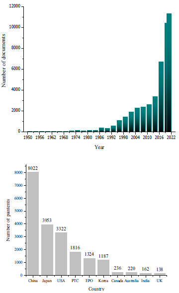
In recent years, perovskites have become a subject of an intense study (Fig. 1. and Fig. 2), with 6000 papers published since 2016. Over the course of the past 87 years, a staggering 105 366 papers have been published on the topic. Only in 2021, approximately 12 000 documents were published, primarily scientific articles (90%), conference proceedings, and reviews. These publications focus on development of different types of perovskites, including their properties, applications, synthesis methods, and composition with other materials (see Table 1 in section 5).
Table 1.
Perovskites composed according to type and application.
Formula |
Supplementary material |
Type |
Application |
Reference |
MAPbI3 |
Textured silicon surface |
organic-inorganic |
Tandem solar cells (TSC) |
[81] |
CsPbBr3 |
Cyclodextrin |
inorganic |
Perovskite nanocrystals |
[82] |
CsPbBr3 |
Cyclodextrin |
inorganic |
Perovskite films |
[83] |
MAPbI3 |
Polylysine (PLL) |
organic-inorganic |
Perovskite films |
[84] |
MAPbI3 |
Starch |
organic-inorganic |
Gravure printing of flexible solar cells |
[85] |
MAPbI3 |
Starch |
organic-inorganic |
Solar cell |
[86] |
MAPbI3 |
Starch |
organic-inorganic |
Solar cell ink |
[87] |
MAPbI3 |
Starch |
organic-inorganic |
Photoactive thin layers for solar cells |
[53] |
MAPbI3 |
Starch |
organic-inorganic |
Flexible solar cells |
[88] |
FAPbI3 |
Starch |
organic-inorganic |
LEDs |
[89] |
MAPbBr3 |
Polyvinylidene fluoride (PVDF) |
organic-inorganic |
MAPbBr3 composite films embedded in PVDF |
[90] |
CsPbBr3 |
Poly(methyl)methacrylate (PMMA) |
inorganic |
Perovskite/PMMA nanocrystal fibres |
[91] |
MAPbBr3 |
Poly(methyl)methacrylate (PMMA) |
organic-inorganic |
Perovskite quantum dots |
[92] |
FASnI3 |
Polystyrene sulfonate (PS) |
lead-free organic |
Solar cells |
[10] |
CsPbBr3 |
Composite glass (GeO2/B2O3/ZnO/CaO/PbO/Cs2O/NaBr) |
inorganic |
Luminescent solar concentrators |
[69] |
MAPbI3 |
Polysilanes |
organic-inorganic |
Solar cells |
[93] |
MAPbI3 |
Polyethylene glycol, polyethylenoimine, poly(acrylic acid) and polyvinylpyrrolidone |
organic-inorganic |
Solar cells |
[94] |
MAPbI3 + NH4Cl |
Willow Glass |
organic-inorganic |
Flexible solar cells |
[95] |
MAPbBr3 |
Poly(L-lactic acid) |
organic-inorganic |
PC-LEDs (light-emitting diodes in remote configuration) |
[96] |
CsPbBr3 |
Poly(methylmethacrylate), poly(butylmethacrylate) (PBMA) and polystyrene |
inorganic |
Rubber discs and cylinders |
[97] |
CsPbBr3 |
poly(maleic anhydride-alt-1-octadecene) (PMMA) |
inorganic |
Light-emitting diodes (LEDs) |
[70] |
CsPbBr3 |
Polysilazane (PSZ) |
inorganic |
W-LEDs (white LEDs) |
[98] |
Moreover, the majority of these documents fall under the umbrella of materials science, with 68 682 papers and a 30% participation rate. Physics and astronomy follow closely behind at 22%, while chemistry and engineering make up 16% and 14%, respectively. Other topics such as environment, biochemistry, and energy occupy the remaining percentage. This means that perovskites are one of the most important research topics of the 21st century. The focus is primarily on the elaboration and characterisation of materials with high-energy efficiency, with the goal of applying perovskites to engineering and industrial-level mechanisms. As such, it is an area of research that has farreaching implications for a broad range of industries and scientific disciplines.
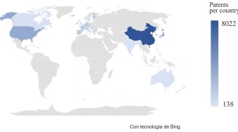
Now, knowing the publications trends of papers on perovskites over time, according to the data presented in Figs. 1 and 2, it is possible to find trends of the countries where the largest number of patents are produced. China is leading the pack with the highest number of patents produced. However, it is important to note that Japan and the United States have also made significant contributions in solving various challenges associated with perovskites such as: formation of some types of perovskites, creating manufacturing methodologies at industrial level and synthesizing nanocrystals that remain stable to exposure from different media. On the other hand, countries like Canada, Australia, India, and the United Kingdom have not made significant contributions to this field. These countries barely occupy 1% each with respect to the total number of patents created. However, it is important to note that research in this field is still ongoing and there is a lot of potential for these countries to make significant contributions in the future.
General crystal system of perovskites
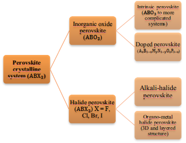
Perovskites main formula is ABX3, where A and B are cations of different volumes, X can be oxygen, metal halides, sulphides or nitrides [13, 28, 29]. These materials can be classified into two main groups: perovskites of inorganic oxide where X is the oxygen (ABO3) and perovskites of metal halides where X is the halide within the metal halides group. There are also the perovskites of alkaline halide and the perovskite of organometallic halide (Fig. 3).
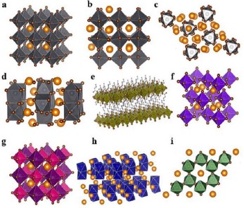
Their crystal structure is divided into four types based on their octahedral coordination: zero-dimensional (0D), one-dimensional (1D), two-dimensional (2D), and three-dimensional (3D) [17, 31]. Nevertheless, 2D and mixed 2D–3D halide perovskites stand out for their optoelectronic properties [32]. These structures are shown in Fig. 4.
Metal halide perovskites
Metal halide perovskites are a type of semiconductor with remarkable optoelectronic properties. Their chemical formula, ABX3, reveals that they are composed of A as an organic or inorganic cation (MA, FA, Cs), B as a metal ion (Pb, Sn, Bi), and X as a halide or halide mixture (I, Br, Cl, I–Br) [9]. This unique combination results in an octahedral coordination and a 3D crystal structure [31]. By varying the components A, B, and X, different types of perovskites can be synthesized, each with their own distinct properties. This versatility allows for the selection of the most appro-priate perovskite crystals for specific applications [34], such as fabrication of high-performance optoelectronic devices, including solar cells, photodetectors and ionizing radiation detectors, LEDs, and lasers. They have also been used in the fields of memory and solar energy conversion into fuel [35, 36].
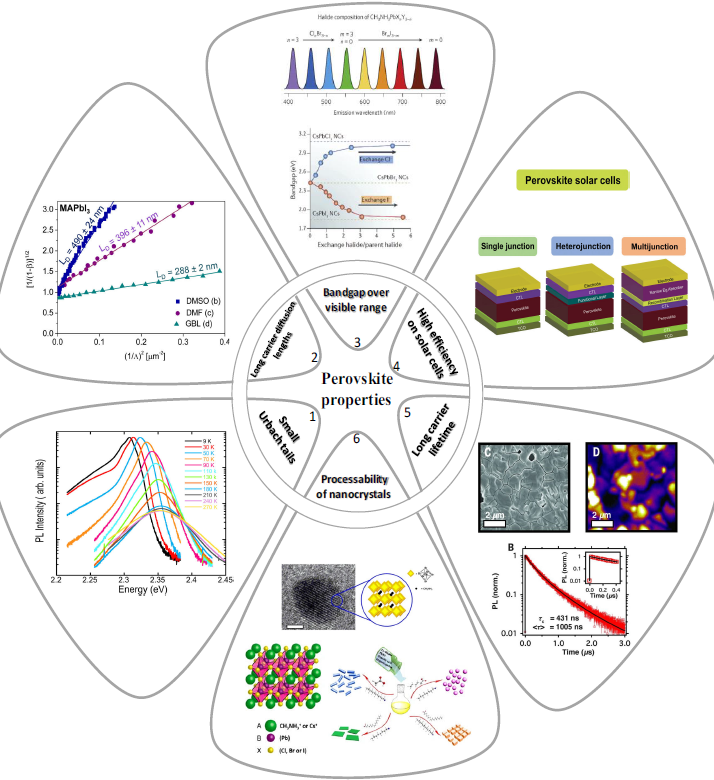
Fig. 5 illustrates some of the main properties of perovskite semiconductors:
- The sharp absorption orders show small Urbach tails, indicating a small contribution from static disorder. The amplitude of these tails depends on the interaction between excitons and photons [37].
- The diffusion length of the metal halide perovskite MAPbI3 prepared in different solvents: DMSO (dimethyl sulfoxide), DMF (N,N-dimethylformamide), and GBL (Butyrolactone) shows that dimethyl sulfoxide produces the longest wave-length of 490 nm, indicating a longer lifetime for semi-conductor matter [38].
- In the visible spectrum emission range, perovskite semiconductors present a direct energy gap with high photoluminescence quantum yield and narrow bandwidth [34].
- Perovskite solar cells have different joint configurations, including one union, hetero unions, and multiple unions. This is how it has been discovered that heterojunction structures suppress carrier recombination while multijunction structures reduce losses by thermalization [39].
- According to DeQuilettes et al. in 2015, the lifetime of perovskite carriers can reach up to 250 ns or more, which is a measure of the film quality [40].
- one of the most striking properties of perov-skites is their processability. Different characteristics such as optics can be modified by varying the composition of halide ions and cations. The size and dimensions of the crystals can also be adjusted. For example, inorganic perov-skites can undergo dimensional transformation by varying the ligands used in the synthesis [41]
There are various methods for the in situ deposition of perovskite films, including spin coating, dip coating, inkjet printing, direct deposition on substrate, double-source co-evaporation, and vapour-assisted solution. Among these, the vapour-assisted solution technique is one of the most recent and widely used [42–46]. The selection of the deposition technique depends on the solution nature, such as its density, viscosity, and homogeneity, as well as availability of equipment. Some techniques allow deposition under ambient conditions using "green" solvents and antisolvents. These types of solvents are characterised by being safe and sustainable substances that replace traditional solvents, which tend to be toxic and harmful to the environment. Green solvents have attracted the attention of the scientific community because they facilitate the transition from laboratory-scale syntheses to industrial-scale processes [47, 48].
Particularly, the aerosol-assisted chemical vapour depo-sition technique is a promising method that can be carried out under ambient atmospheric conditions. This process involves exposing the substrate to inorganic perovskite vapours at high temperatures, achieving uniform coverage and allowing the use of green solvents such as water and antisolvents such as alcohols. In this sense, for the first time Becerril et al. developed a single-source chemical vapour deposition coating process for glass substrates, where water was used as the only solvent for inorganic perovskite precursors CsPbCl3 and green antisolvents propan-2-one, propan-2-ol, methanol, and ethanol. Films without signs of oxidation or degradation were obtained, finding that anti-solvents with high boiling point and low ΔcH° liquid generate higher quality films. This can be attributed to heterogeneous nucleation and preferential crystal orienta-tion, resulting in more compact films with higher coverage. As a result, photoluminescence of up to 91.44% was reported with ethanol, and the obtained materials presented a charac-teristic exitonic transition of the perovskite at 418 nm [49].
Organic-inorganic hybrid metal halide perovskites
From this type of perovskites, films can be synthesized because they combine plastic mechanical properties (organic) and electronic mobility (inorganic) in their configuration of ABX3. Having an organic cation A that is usually methylammonium (MA) or formamidinium (FA), a metal ion B that is Pb or Sn, and X that is Cl, Br, or I, which can structurally form in a sixfold coordination surrounded by an octahedron of halide anions together with ammonium cations in a 12-fold cuboctahedral coordination [50, 51]. By combining different A, B, and X components, up to 50 varieties of perovskites can be generated with different properties, making them highly versatile materials increasing the diffusion length of the film and raising the photovoltaic efficiency [38]. These are developed from methods that use annealing temperatures, antisolvent treatment, acceleration of crystallisation, solvent engineering [Fig. 6(d)], among others [52].
One of the most promising applications of perovskites are insular cells. In the last decade, perovskite solar cells have achieved a power conversion efficiency (PCE) of up to 25.5%, surpassing conventional silica cells, using simpler and low-cost processes. However, their thermal stability is limited to only 150° C or even less [53, 54]. To overcome this limitation, researchers have been exploring different methods to synthesize perovskite films, such as annealing temperatures, antisolvent treatment, acceleration of crystallisation, and solvent engineering.
Solvent engineering is a particularly promising technique for synthesizing perovskite films with high PCEs. This method involves using different solvents to control the crystallisation process and generate uniform films with high quality. For example, Jeon et al. in 2014 developed a perovskite cell structure MAPb(I1−xBrx) using methyl-ammonium iodide (MAI), methylammonium bromide (MABr), lead iodide (PbI2) and lead bromide (PbBr2) in the solvents GBL and DMSO applying toluene as an antisolvent with the solvent engineering method [Fig. 6(d)] because the methods usually applied as rotational coating do not produce homogeneous layers with uniform thicknesses. This perovskite film was eventually deposited in a layer of mp-TiO2 on a layer of poly(triarylamine) (PTAA), and gold (Au) [Fig. 6(a)] reaching a conversion efficiency of 16.2%. The bilayer structure, comprising mesoscopic and flat structures, was effective in sufficiently absorbing light and collecting charges, showing promising results for the development of more efficient and cost-effective solar cells in the future [55].
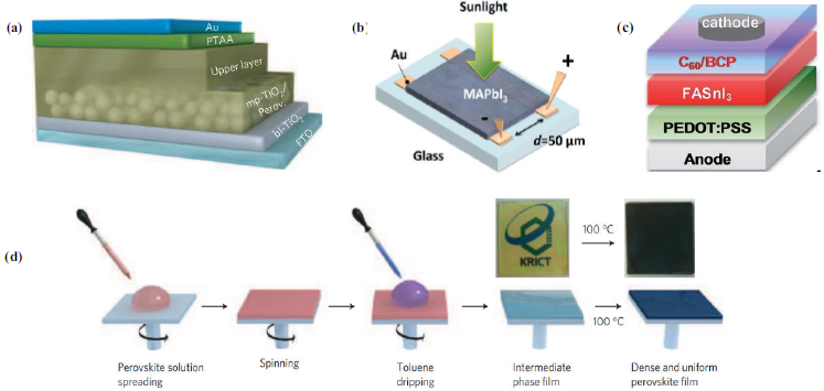
In this sense, to understand the electrical behaviour of the compound MA, one of the most used in hybrid perovskites for different photovoltaic units, Yuan and his team developed lateral structure devices which present a totally different layer configuration to the one presented in Fig. 6(a). The researchers used MAI and PbI2 precursors to synthesize the MAPbI3 perovskite film between two gold (Au) electrodes deposited on a glass substrate by thermal evaporation [Fig. 6(b)]. Through photothermal resonance microscopy (PTIR) and Kelvin probe force microscopy (KPFM), they identified the ion electromigration of methylammonium, which can migrate easily when subjected to an electric field as small as ≈ 0.3 V/μm at room temperature. This discovery sheds light on how the electrical properties of hybrid perovskites can be manipulated [56].
"Lead-free" hybrid perovskites are another type of hybrid perovskites that have emerged due to the toxicity concerns associated with lead-based optoelectronic devices despite the significant advancements made in this field [57, 58]. Compounds such as tin (Sn), germanium (Ge), bismuth (Bi), antimony (Sb), copper (Cu), and titanium (Ti) have been used to produced perovskites with optical and electrical properties comparable to those of lead [10, 59]. These advancements are crucial in mitigating the environmental impact of lead-based optoelectronic devices.
However, some of these lead-free perovskites have very low PCEs due to the high background carrier density caused by intrinsic defects such as vacancies and oxidised and highly unstable species in air [17, 60]. To address this issue, researchers have been exploring various approaches. One such approach is the rotational coating process which was employed by Shao et al. in 2018 to synthesize a thin layer of FASnI3 perovskite (formamidinium tin iodide) through the rotational coating process. By mixing solvents such as DMSO and DMF and using ethyl ether as an antisolvent, they were able to reduce the density of back-ground carriers. It was deposited with the orthorhombic a-axis in the direction outside the plane and adding traces of 2D tin perovskite [Fig. 6(c)], resulting in a PCE of up to 9% [61].
In contrast, Cortecchia and his team developed MA2CuClxBr4−x perovskites to reduce the instability associated with tin perovskites. They used spin coating to form stable nanocrystals and suitable for optoelectronic applications and found that the optical properties depend on Cu, but mainly on the Br/Cl ratio because the intensity of a green photoluminescence at 515 nm increased with a greater amount of this ratio [62].
Inorganic metal halide perovskites
This type of Perovskites was reported in 1893, but it was not until the 1990s that their optical and electronic properties were utilized in light-emitting devices. Initially, they were used as sensitizing materials for solar cells, but it was discovered that they were also ideal for charge transport and light generation. In recent years, the focus has been on improving quantum photoluminescence yields, accessing to the confined quantum size regime to tune emission, and increasing PCE [33, 63, 64]. To meet these requirements, perovskites are elaborated from the mono-valent inorganic cation caesium (Cs) which satisfies the base configuration of perovskites forming CsBX3 structures. These inorganic metal halide perovskites are more stable than those based on organic elements, with yields up to 21% and thermal stability (CsPbBr3 is stable above 500 °C compared to MAPbBr3 that is up to 432 °C) and adequate emission ranges [65–68]. This is how they can be classified into alkali metal halide perovskites, transitional, and lead-based or "lead-free" perovskites.
Lead-containing substance: surprisingly, caesium-based (Cs) lead halide quantum dots have replaced group II-VI semiconductor materials due to their superior photo-luminescence properties, becoming potential candidates for applications such as LEDs, lasers, photodetectors, non-linear, solar cells, and as spectrochemical probes to detect ions [68–70].
Specifically, perovskites with CsPbBr3 structure are inorganic and come from CsBr and PbBr2 precursors. These materials possess a visible green range from 20 nm to 520 nm [67, 71, 72] and have been found to exhibit properties such as surface roughness, ink stability, and high thermal and environmental stability. These unique characteristics have allowed for a development of efficient devices and technology. They are generally obtained through hot injection and LARP methods [26, 36, 73]. According to Ng (2020), solvents such as toluene, low-polarity antisolvents like ethyl acetate, and ligands such as oleylamine are required for the synthesis of these materials [25]. Additionally, Swarnkar et al. developed PeLEDS (totally inorganic perovskite LEDs processed in solution) of caesium lead bromide perovskite with phenethyl-ammonium additives (PEABr). This technique has resulted in crystals with reduced sizes (< 15 nm) and efficient energy channelling and dielectric additive polyethylene glycol (PEG), resulting in compact films and passivation of defects in the limits of the grains, reaching an external quantum efficiency of 13.14% [74].
Lead-free metal halides: in these lead-free hybrid perovskites, the fundamental structure consists of B being a metal ion such as germanium (Ge) or tin (Sn), and methods have been developed to replace Pb with a monovalent and trivalent metal cation forming ordered double perovskites [59, 75, 76]. This is the case of Zhou and his team who synthesized Cs2AgBiBr6 perovskites through a hot- injection method [Fig. 7(a)] to reduce the volatility towards humidity, air or lighting that tin perovskites present. These nanocrystals are stable for almost three weeks and have moisture resistance of 55%, making them suitable for optoelectronic or photocatalytic applications. However, their PCE values are only around ~1% [77].
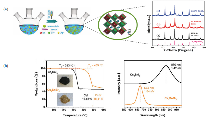
Similarly, McClure et al. elaborated double perovskites with bromine halides and chlorine (Cs2SnBr6 and Cs2SnCl6) which have shown that both components adopt a double cubic structure and reflect bandgaps of 2.19 and 2.77 eV, respectively, comparable to those obtained in lead-based hybrid perovskites. However, they present some problems that need to be overcome, such as indirect bandgaps due to the interaction between the 4d orbitals of Ag and the 3p/4p orbitals of the halide ion that modify the valence band [60]. In contrast, there are tin perovskites with Cs2SnX6 structure which have achieved thermal stability of up to 313 °C, as reported by Han et al. They synthesized perovskites based on iodine and bromine halides (Cs2SnI6 and Cs2SnBr6) which exhibited bandgaps of 1.84 and 1.42 eV, respectively [Fig. 7(b)]. These results suggest that both materials hold promise for optoelectronic applications [54].
Compound perovskites
The incorporation of other materials into hybrid or inorganic perovskites (Table 1), as revealed by the research discussed above, is driven by the need to maintain the stability of their structure and properties under various environmental conditions, such as exposure to air, humidity, and thermal stress, and to enable the transition from laboratory-scale processes to industrial-scale production. This approach has led to the development of various devices and technologies, such as inks for solar cells, photovoltaic units, different types of LEDs, films, perovskite fibres and others, where polymers and biopolymers (Fig. 8) are often added to perovskite arrays to produce defect-free films with larger cell sizes [78–80].
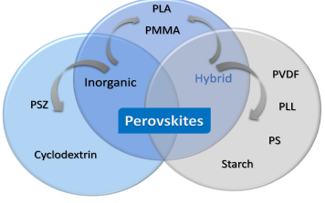
Application with polymers
In recent years, engineering strategies have been developed to enhance the stability of perovskites. One of these strategies involves encapsulating nanocrystals within polymeric protective matrices, such as PS, PMMA, PSZ, PBMA, and PVDF using single-step electrospinning techniques or ligands. In this approach, crystals grow inside polymer fibres and are encapsulated in the polymer matrix, resulting in uniform sizes and spatial distributions of the crystals [72, 98]. For example, in LEDs, quantum photo-luminescence yields of 40% have been achieved using this method, and 70% of this yield has been retained after immersion in water for 192 h and 50% after exposure to 80 °C for 120 min. This approach has enabled various applications, although there are still issues such as limited service life [70].
Another application is the production of different structures, such as discs and cylinders, with controlled optoelectronic and mechanical properties (rigidity and flexibility), generated by the formation of perovskite crystals and polymer matrix in a single reaction, obtaining photo-luminescence quantum yields (PLQYs) of over 60% [97].
Application with biopolymers
As an alternative to using polymers derived from hydrocarbons, the composition of perovskites with organic materials has been explored, due to their environmental compatibility and abundance. Various advantages and properties have been observed when implementing materials such as starch, cyclodextrins, polylactic acid and PLL in LED optoelectronic devices and photovoltaic units.
Starch
The first starch-based perovskites (derived from corn) were hybrid perovskites (MAPbI3 and FAPbI3) synthesized in DMSO, as this polysaccharide is not soluble in conventional organic solvents except for DMSO [99], which can form inclusion complexes with fatty acids and other ligands [100]. This allows the process to be carried out without toxic antisolvents, facilitating the transition from laboratory processes to commercial production. Starch acts as a rheological modifier that increases viscosity and gelatinization enhances the interaction between the –OH groups of starch and perovskite precursors. This method has PCEs of up to 17.2% with improved stability in humid environments (50%) for more than 800 h [86], resulting in flexible devices that can be shaped according to the application.
Leoncini et al. [53] found that the biopolymer affects charge traps and ionic mobility which require higher activation energy, but still retain the ambipolar charge transport nature and the same mobility values of perovskite. This suggests that starch acts as mechanical reinforcement. In this way, it has been possible to produce inks for solar cells, LEDs, and flexible solar cells in roll through processes such as gravure printing [86, 88, 89].
Cyclodextrins
Inorganic CsPbBr3 perovskite precursors have been mixed with cyclodextrins (a-CD and b-CD) to replace the ligands in the LARP method, achieving the formation of crystals and smooth films through ultrasonication that are stable when exposed to moisture and light. This is due to the strong coordination of the hydroxyl groups of cyclodextrins with lead metal ions, which allows the encapsulation of the nanocrystals. Compared to perovskites obtained through oleic acid and oleylamine, perovskites produced using cyclodextrins exhibited higher productivity, higher quantum yield of photoluminescence (85%), and greater resistance to moisture, heat and laser irradiation. However, nanocrystals remain unstable in aqueous solutions, possibly due to the formation of networks through hydrogen bounding, unlike perovskite films, which are super luminescent, stable and promising for possible applications in optoelectronic devices [82, 83].
Polylactic acid and polylysine
Polylactic acid (PLA) and polylysine (PLL) have been used as environmentally-friendly and cost-effective natural additives in the synthesis of perovskites to passivate defects in perovskite films. In general, the incorporation of a hydrophobic polymer that acts as a barrier against moisture helps improve stability and, if possible, controls grain size. This has led to the development of various technologies, including solar cells with PLL and hybrid methylammonium perovskites reaching a PCE of 19.45% [84].
On the other hand, PLA has been used to produce PC-LEDs (LEDs in remote configuration) and WLEDs from inorganic perovskites of caesium bromide and lead using the in situ LARP process. In this approach, the polymer acting as a matrix and the perovskite serving as an emitter obtained quantum yields of photoluminescence higher than 85%, operational stability of 600 h, stability under environ-mental storage, water, and thermal stress [96].
Discussion
Research on materials, such as perovskites, has been growing exponentially in recent years because it is a material with optical and electronic potential, which has advantages over those that have already been studied and used for applications such as LEDs and solar cells semiconductors such as silicon.
These advantages, as reviewed, in the first place are the variety of structures, colours, and raw materials with which they can be manufactured, solving problems such as obtaining monochromatic white light LEDs, covering the different colour ranges of lasers, among others. Secondly, they have high yields with simple, low-cost, and accessible materials which allow scaling up their production to an industrial level. Thirdly, they have optimal and acceptable properties to produce solar cells as efficient as traditional ones, one of the most recent being hetero- and multi-junction solar cells which have been able to increase the PCE by up to 430%.
However, there are still problems that prevent their complete commercialization, some of which are their stability and efficiency over time, the use of large quantities of highly toxic solvents and the application of lead in their base structure. It should be noted that some solutions have been generated for these problems, such as lead-free perovskites and the use of polymers to contain them, among others.
Conclusions
The research carried out is a review about the evolution of perovskites from their origins to the application of metal halides in the base cubic structure ABX3 for hybrid and organic perovskites, as well as trends in material engi-neering of perovskites composed of polymers and biopolymers. Perovskites have attracted great interest as a material for the development of energy-efficient devices, particularly in the last decade and in countries such as China, Japan, and the United States. Their optical and electronic transfer characteristics, simple synthesis processes, and low cost have led to laboratory-scale studies to test different synthesis methods (LARP, hot injection, ultrasonication, electro spinning, among others), characterise and classify the variety of structures in which they can be developed and study their properties and interaction with other materials. The goal is to improve their stability, so that they can be applied at an industrial level and exposed to the environment without compromising their efficiency. Therefore, perovskites have emerged from hybrid and inorganic metal halides which have similar properties but different efficiencies and stability. This is how interactions with other materials have been explored to address these problems.
Perovskites composed of polymers and biopolymers have improved stability in environment conditions such as humidity and temperature, enabling the development of flexible devices in various sizes and shapes for application in solar cells, laser, LEDs of different types and inks. In addition, natural polymers such as starch and hybrid perovskites have enabled the development of processes free of antisolvents, which are highly toxic, making it possible to approach the manufacture of these technologies at an industrial level. However, the current challenges are focused on improving the efficiency of these compound perovskites so that they can even surpass conventional technologies through sustainable processes consistent with the objectives of sustainable development. In the future, interactions between inorganic perovskites (with electrical properties) exhibiting greater stability and organic materials repre-senting the mechanical structure, such as cellulose or the combination of starches from other types of sources (plants, tubers, and fruits), can be studied.
Authors’ statement
H.F. performed writing of the original draft and conceptualization; K.R. designed the methodology and review editing; H.C. performed supervision and project administration.
Acknowledgements
The authors would like to thank the call #19-2021 with the SGI 3249 project, as well as Universidad Pedagógica y Tecnológica de Colombia and the research group GITYD of the same institution.
References
-
Strielkowski, W., Veinbender, T., Tvaronavičienė, M. & Lace, N. Economic efficiency and energy security of smart cities. Econ. Res.- Econ, Istraz. 33, 788–803 (2020). https://doi.org/10.1080/1331677X.2020.1734854
-
Khan, I. & Halder, P. K. Electrical energy conservation through human behavior change: Perspective in Bangladesh. Int. J. Renew. Energy Res. 6, 43–52 (2016). https://doi.org/10.20508/ijrer.v6i1.3030.g6758
-
Rehman, A., Rauf, A., Ahmad, M., Chandio, A. A. & Deyuan, Z. The effect of carbon dioxide emission and the consumption of electrical energy, fossil fuel energy, and renewable energy, on economic performance: evidence from Pakistan. Environ. Sci. Pollut. Res. 26, 21760–21773 (2019). https://doi.org/10.1007/s11356-019-05550-y
-
John, S. V. Next generation bulk heterojunction organic photo- voltaic and light emitting diode sytems of novel polycyclic aromatic hydrocarbon. (University of the Western Cape, 2017). John_PhD_NSC_2017.pdf
-
AL Shaqsi, A. Z., Sopian, K. & Al-Hinai, A. Review of energy storage services, applications, limitations, and benefits. Energy Rep. 6, 288–306 (2020). https://doi.org/10.1016/J.EGYR.2020.07.028
-
Ellis, E. V, Gonzalez, E. W., Kratzer, D. A., McEachron, D. L. & Yeutter, G. Auto-Tuning Daylight with Leds: Sustainable Lighting for Health and Wellbeing. in 2013 ARCC Architectural Research Conference 465–473 (University of North Carolina, 2013). https://www.brikbase.org/sites/default/files/ARCC2013_UNCC_Conference_Proceedings_483.pdf
-
Ahmad, A. S. et al. A review on applications of ANN and SVM for building electrical energy consumption forecasting. Renew. Sust. Energ. Rev. 33, 102–109 (2014).https://doi.org/10.1016/j.rser.2014.01.069
-
Zissis, G., Bertoldi, P. & Serrenho, T. Update on the Status of LED- Lighting World Market Since 2018. (JRC Technical Report). (European Union Publications Office, Luxembourg, 2021) https://data.europa.eu/doi/10.2760/759859
-
Zhang, W., Eperon, G. E. & Snaith, H. J. Metal halide perovskites for energy applications. Nat. Energy 1, 1–17 (2016). https://doi.org/10.1038/nenergy.2016.48
-
Chen, K. et al. Low-dimensional perovskite interlayer for highly efficient lead-free formamidinium tin iodide perovskite solar cells. Nano Energy 49, 411–418 (2018). https://doi.org/10.1016/j.nanoen.2018.05.006
-
Soe, C. M. M. Emerging three-dimensional and two-dimensional hybrid halide perovskites: from synthesis to thin film properties and solar cell performance. (Northwestern University, 2017).https://doi.org/10.21985/N2Q16N
-
Qi, W. et al. Inorganic material passivation of defects toward efficient perovskite solar cells. Sci. Bull. 65, 2022–2032 (2020). https://doi.org/10.1016/j.scib.2020.07.017
-
Assirey, E. A. R. Perovskite synthesis, properties and their related biochemical and industrial application. Saudi Pharm. J. 27, 817–829 (2019). https://doi.org/10.1016/j.jsps.2019.05.003
-
Aftab, S., Nawaz, T. & Bilal Tahir, M. Recent development in shape memory based perovskite materials for energy conversion and storage applications. Int. J. Energy Res. 45, 20545–20558 (2021). https://doi.org/10.1002/er.7151
-
Jena, A. K., Kulkarni, A. & Miyasaka, T. Halide perovskite photo- voltaics: background, status, and future prospects. Chem. Rev. 119, 3036–3103 (2019). https://doi.org/10.1021/acs.chemrev.8b00539
-
Choithrani, R. Analysis of Thermodynamic and Phononic Properties of Perovskite Manganites. in Magnetic Sensors Principles and Applications (Ed. Kuang, K.) 3–18 (IntechOpen, 2012). https://doi.org/10.5772/33872
-
Fan, Q. et al. Lead-free halide perovskite nanocrystals: crystal structures, synthesis, stabilities, and optical properties. Angew. Chem. Int. Ed. 59, 1030–1046 (2020). https://doi.org/10.1002/anie.201904862
-
Duan, Y., Wang, D. Y. & Costa, R. D. Recent progress on synthesis, characterization, and applications of metal halide perovskites@metal oxide. Adv. Funct. Mater. 31, 2104634 (2021). https://doi.org/10.1002/adfm.202104634
-
Cranford, S. The real power of perovskite progression. Matter 4, 3787–3789 (2021). https://doi.org/10.1016/j.matt.2021.10.028
-
Katz, E. A. Perovskite: Name puzzle and german-russian odyssey of discovery. Helv. Chim. Acta 103, e2000061 (2020). https://doi.org/10.1002/hlca.202000061
-
Mitzi, D. B. Introduction: perovskites. Chem. Rev. 119, 3033–3035 (2019). https://doi.org/10.1021/ACS.CHEMREV.8B00800
-
Lei, Y. et al. A fabrication process for flexible single-crystal perovskite devices. Nature 583, 790–795 (2020). https://doi.org/10.1038/s41586-020-2526-z
-
Karim, M. A., Biswas, S. K. & Rahman, M. A. Investigation of the Electrical, Optical & Structural Characteristics of Mixed Halide Perovskite Thin Films. in 5th Int. Conf. Comput. Commun. Chem. Mater. Electron. Eng. (IC4ME2) 10–14 (IEEE, 2019). https://doi.org/10.1109/IC4ME247184.2019.9036643
-
Wei, Y., Cheng, Z. & Lin, J. Correction: An overview on enhancing the stability of lead halide perovskite quantum dots and their applications in phosphor-converted LEDs. Chem. Soc. Rev. 48, 405 (2019). https://doi.org/10.1039/c8cs00740c
-
Ng, C. K., Yin, W., Li, H. & Jasieniak, J. J. Scalable synthesis of colloidal CsPbBr3 perovskite nanocrystals with high reaction yields through solvent and ligand engineering. Nanoscale 12, 4859–4867 (2020). https://doi.org/10.1039/C9NR10726F
-
Xu, D. et al. Enhancing the performance of LARP-synthesized CsPbBr3 nanocrystal LEDs by employing a dual hole injection layer. RSC Adv. 10, 17653–17659 (2020). https://doi.org/10.1039/d0ra02622k
-
Deng, J., Xun, J. & He, R. Facile and rapid synthesis of high performance perovskite nanocrystals CsPb(X/Br)3 (X = Cl, I) at room temperature. Opt. Mater. 99, 109528 (2020). https://doi.org/10.1016/j.optmat.2019.109528
-
Moure, C. & Peña, O. Recent advances in perovskites: Processing and properties. Prog. Solid State Ch. 43, 123–148 (2015). https://doi.org/10.1016/j.progsolidstchem.2015.09.001
-
Williams, A. E. et al. Perovskite processing for photovoltaics: a spectro-thermal evaluation. J. Mater. Chem. A 2, 19338–19346 (2014). https://doi.org/10.1039/C4TA04725G
-
Gao, P., Grätzel, M. & Nazeeruddin, M. K. Organohalide lead perovskites for photovoltaic applications. Energy Environ. Sci. 7, 2448–2463 (2014). https://doi.org/10.1039/C4EE00942H
-
Zeng, Z. et al. Rare-earth-containing perovskite nanomaterials: Design, synthesis, properties and applications. Chem. Soc. Rev. 49, 1109–1143 (2020). https://doi.org/10.1039/c9cs00330d
-
Kim, E. B. et al. A review on two-dimensional (2D) and 2D-3D multi- dimensional perovskite solar cells: Perovskites structures, stability, and photovoltaic performances. J. Photochem. Photobiol. C 48, 100405 (2021). https://doi.org/10.1016/j.jphotochemrev.2021.100405
-
Shamsi, J., Urban, A. S., Imran, M., De Trizio, L. & Manna, L. Metal halide perovskite nanocrystals: synthesis, post-synthesis modifi- cations, and their optical properties. Chem. Rev. 119, 3296–3348 (2019). https://doi.org/10.1021/acs.chemrev.8b00644
-
Ou, Q. et al. Band structure engineering in metal halide perovskite nanostructures for optoelectronic applications. Nano Mater. Sci. 1, 268–287 (2019). https://doi.org/10.1016/j.nanoms.2019.10.004
-
Mao, W. et al. Controlled growth of monocrystalline organo-lead halide perovskite and its application in photonic devices. Angew. Chem. Int. Ed. 56, 12486–12491 (2017). https://doi.org/10.1002/anie.201703786
-
Kulkarni, S. A., Mhaisalkar, S. G., Mathews, N. & Boix, P. P. Perovskite nanoparticles: synthesis, properties, and novel applica- tions in photovoltaics and leds. Small Methods 3, 1800231 (2019). https://doi.org/10.1002/smtd.201800231
-
Falsini, N. et al. Analysis of the Urbach tail in cesium lead halide perovskites. J. Appl. Phys. 131, (2022). https://doi.org/10.1063/5.0076712
-
Adhyaksa, G. W. P. et al. Carrier diffusion lengths in hybrid perovskites: processing, composition, aging, and surface passivation effects. Chem. Mater. 28, 5259–5263 (2016). https://doi.org/10.1021/acs.chemmater.6b00466
-
Wu, X., Li, B., Zhu, Z., Chueh, C. & Jen, A. K. Y. Designs from single junctions, heterojunctions to multijunctions for high- performance perovskite solar cells. Chem. Soc. Rev. 50, 13090– 13128 (2021). https://doi.org/10.1039/d1cs00841b
-
DeQuilettes, D. W. et al. Impact of microstructure on local carrier lifetime in perovskite solar cells. Science 348, 683–686 (2015). https://doi.org/10.1126/science.aaa5333
-
Huang, H. et al. Colloidal lead halide perovskite nanocrystals: Synthesis, optical properties and applications. NPG Asia Mater. 8, e328 (2016). https://doi.org/10.1038/am.2016.167
-
Chen, W. et al. A semitransparent inorganic perovskite film for overcoming ultraviolet light instability of organic solar cells and achieving 14.03% efficiency. Adv. Mater. 30, 1800855 (2018). https://doi.org/10.1002/adma.201800855
-
Leyden, M. R., Jiang, Y. & Qi, Y. Chemical vapor deposition grown formamidinium perovskite solar modules with high steady state power and thermal stability. J. Mater. Chem. A 4, 13125–13132 (2016). https://doi.org/10.1039/C6TA04267H
-
Jarernboon, W. et al. The effects of csbr concentration on the inorganic cesium lead bromide perovskite film properties and the performances of carbon-based HTM-free perovskite solar cells. Curr. Appl. Sci. Technol. 22, 1–13 (2021). https://doi.org/10.55003/cast.2022.05.22.003
-
Rico-Yuson, C. A., Danwittayakul, S., Kumar, S., Hornyak, G. L. & Bora, T. Sequential dip-coating of CsPbBr3 perovskite films in ambient conditions and their photovoltaic performance. J. Mater. Sci. 57, 10285–10298 (2022). https://doi.org/10.1007/s10853-022-07299-1
-
Cohen, T. A. et al. Direct patterning of perovskite nanocrystals on nanophotonic cavities with electrohydrodynamic inkjet printing. Nano Lett. 22, 5681–5688 (2022). https://doi.org/10.1021/acs.nanolett.2c00473
-
Hoseinpour, V., Shariatinia, Z. & Mahmoodpour, S. Surface passivation boosted performances of perovskite solar cells assembled under ambient conditions. Opt. Mater. 131 , 112746 (2022). https://doi.org/10.1016/j.optmat.2022.112746
-
Baral, P. et al. Efficient and stable perovskite solar cells based on blade-coated CH3NH3PbI3 thin films fabricated using “green” solvents under ambient conditions. Org. Electron. 116, 106763 (2023). https://doi.org/10.1016/j.orgel.2023.106763
-
Becerril, L. et al. Water as the only solvent for CsPbCl3 and NIR- emitting CsPbCl3:Yb3+ films by antisolvent-enhanced crystalli- zation in aerosol-assisted chemical vapor deposition. Adv. Mater.Technol. 8, 2201890 (2023). https://doi.org/10.1002/admt.202201890
-
Schmidt, L. C. et al. Nontemplate synthesis of CH3NH3PbBr3 perovskite nanoparticles. J. Am. Chem. Soc. 136, 850–853 (2014). https://doi.org/10.1021/ja4109209
-
Snaith, H. J. Present status and future prospects of perovskite photovoltaics. Nat. Mater. 17, 372–376 (2018). https://doi.org/10.1038/s41563-018-0071-z
-
Wang, K. et al. A Nonionic and low-entropic MA(MMA)nPbI3-ink for fast crystallization of perovskite thin films. Joule 4, 615–630 (2020). https://doi.org/10.1016/j.joule.2020.01.004
-
Leoncini, M. et al. Electronic transport, ionic activation energy and trapping phenomena in a polymer-hybrid halide perovskite composite. J. Sci.-Adv. Mater. Dev. 6, 543–550 (2021). https://doi.org/10.1016/j.jsamd.2021.07.006
-
Han, X. et al. Lead-free double perovskite Cs2SnX6: facile solution synthesis and excellent stability. Small 15, 1–7 (2019). https://doi.org/10.1002/smll.201901650
-
Jeon, N. J. et al. Solvent engineering for high-performance inorganic-organic hybrid perovskite solar cells. Nat. Mater. 13, 897– 903 (2014). https://doi.org/10.1038/nmat4014
-
Yuan, Y. et al. Photovoltaic switching mechanism in lateral structure hybrid perovskite solar cells. Adv. Energy Mater. 5, 1500615 (2015). https://doi.org/10.1002/aenm.201500615
-
Yang, L. et al. Perovskite lead-free dielectrics for energy storage applications. Prog. Mater. Sci. 102, 72–108 (2019). https://doi.org/10.1016/j.pmatsci.2018.12.005
-
Ke, W. & Kanatzidis, M. G. Prospects for low-toxicity lead-free perovskite solar cells. Nat. Commun. 10, 1–4 (2019). https://doi.org/10.1038/s41467-019-08918-3
-
Lei, H., Hardy, D. & Gao, F. Lead-free double perovskite cs2agbibr6: fundamentals, applications, and perspectives. Adv. Funct. Mater. 31, 2105898 (2021). https://doi.org/10.1002/adfm.202105898
-
McClure, E. T., Ball, M. R., Windl, W. & Woodward, P. M. Cs2AgBiX6 (X = Br, Cl): new visible light absorbing, lead-free halide perovskite semiconductors. Chem. Mater. 28, 1348–1354 (2016). https://doi.org/10.1021/acs.chemmater.5b04231
-
Shao, S. et al. Highly reproducible sn-based hybrid perovskite solar cells with 9% efficiency. Adv. Energy Mater. 8, 1702019 (2018). https://doi.org/10.1002/aenm.201702019
-
Cortecchia, D. et al. Lead-free MA2CuClxBr4-x hybrid perovskites.Inorg. Chem. 55, 1044–1052 (2016).<https://doi.org/10.1021/acs.inorgchem.5b01896
-
Cheng, L.-P. et al. Efficient CsPbBr3 Perovskite light-emitting diodes enabled by synergetic morphology control. Adv. Mater. 7, 1– 24 (2019). https://doi.org/10.1002/adom.201801534
-
Konstantakou, M., Perganti, D., Falaras, P. & Stergiopoulos, T. Anti-solvent crystallization strategies for highly efficient perovskite solar cells. Crystals 7, 1–21 (2017). https://doi.org/10.3390/cryst7100291
-
Tian, J. et al. Inorganic halide perovskite solar cells: progress and challenges. Adv. Energy Mater. 10, 2000183 (2020) . https://doi.org/10.1002/aenm.202000183
-
Chen, W. et al. Surface reconstruction for stable monolithic all- inorganic perovskite/organic tandem solar cells with over 21% efficiency. Adv. Funct. Mater. 32, 2109321 (2022). https://doi.org/10.1002/ADFM.202109321
-
Ding, Y. et al. A low-cost hole transport layer enables Cspbi2br single-junction and tandem perovskite solar cells with record efficiencies of 17.8% and 21.4%. Nano Today 46, 101586 (2022). https://doi.org/10.1016/j.nantod.2022.101586
-
Ananthakumar, S., Kumar, J. R. & Babu, S. M. Cesium lead halide (CsPbX 3 , X = Cl, Br, I) perovskite quantum dots-synthesis, properties, and applications: a review of their present status. Proc.SPIE 6, 042001 (2016). https://doi.org/10.1117/1.jpe.6.042001
-
Hu, Y., Zhang, W., Ye, Y., Zhao, Z. & Liu, C. Femtosecond-laser- induced precipitation of CsPbBr3 perovskite nanocrystals in glasses for solar spectral conversion. ACS Appl. Nano Mater. 3, 850–857 (2020). https://doi.org/10.1021/acsanm.9b02362
-
Meyns, M. et al. Polymer-enhanced stability of inorganic perovskite nanocrystals and their application in color conversion leds. ACS Appl. Mater. Interfaces 8, 19579–19586 (2016). https://doi.org/10.1021/acsami.6b02529
-
Kovalenko, M. V., Protesescu, L. & Bodnarchuk, M. I. Properties and potential optoelectronic applications of lead halide perovskite nanocrystals. Science 358, 745–750 (2017). https://doi.org/10.1126/science.aam7093
-
Liao, H. et al. A general strategy for in situ growth of all-inorganic CsPbX3 (X = Br, I, and Cl) perovskite nanocrystals in polymer fibers toward significantly enhanced water/thermal stabilities. Adv.Opt. Mater. 6, 1–8 (2018). https://doi.org/10.1002/adom.201800346
-
Solari, S. F., Kumar, S., Jagielski, J. & Shih, C. J. Monochromatic LEDs based on perovskite quantum dots: Opportunities and challenges. J. Soc. Inf. Disp. 27, 667–678 (2019). https://doi.org/10.1002/jsid.834
-
Swarnkar, A. et al. Colloidal CsPbBr3 Perovskite nanocrystals: luminescence beyond traditional quantum dots. Angew. Chem. Int.Ed. 54, 15424–15428 (2015). https://doi.org/10.1002/anie.201508276
-
Mao, X. et al. First-principles screening of all-inorganic lead-free ABX3 perovskites. J. Phys. Chem. C 122, 7670–7675 (2018). https://doi.org/10.1021/acs.jpcc.8b02448
-
Shil, S. K. et al. Crystalline all-inorganic lead-free Cs3Sb2I9 perovskite microplates with ultra-fast photoconductive response and robust thermal stability. Nano Res. 14, 4116–4124 (2021). https://doi.org/10.1007/s12274-021-3351-x
-
Zhou, L., Xu, Y.-F., Chen, B.-X., Kuang, D.-B. & Su, Ch.-Y.Synthesis and photocatalytic application of stable lead-free Cs2AgBiBr6 perovskite nanocrystals. Small 14, 1–7 (2018). https://doi.org/10.1002/smll.201703762
-
Mathies, F., List-Kratochvil, E. J. W. & Unger, E. L. Advances in inkjet-printed metal halide perovskite photovoltaic and optoelectronic devices. Energy Technol. 8, 1900991 (2020). https://doi.org/10.1002/ente.201900991
-
Wang, Y. et al. Ultrastable, highly luminescent organic-inorganic perovskite - polymer composite films. Adv. Mater. 28, 10710–10717 (2016). https://doi.org/10.1002/adma.201603964
-
Han, T. H. et al. Perovskite-polymer composite cross-linker approach for highly-stable and efficient perovskite solar cells. Nat. Commun. 10, 520 (2019). https://doi.org/10.1038/s41467-019-08455-z
-
Wang, J. et al. Simple solution-processed approach for nanoscale coverage of perovskite on textured silicon surface enabling highly efficient perovskite/si tandem solar cells. Energy Technol. 9, 2000778 (2021). https://doi.org/10.1002/ente.202000778
-
Guo, F., Wang, Y. Y., Zhang, J., Wei, X. L. & Mo, Z. H.Cyclodextrin-mediated colloidal synthesis of highly luminescent and stable CsPbBr3perovskite nanocrystals. New J. Chem. 44, 17368–17373 (2020). https://doi.org/10.1039/d0nj03772a
-
Zhou, Z. K., Mo, Z. H. & Wei, X. L. Higher quantum efficiency and moisture resistance of all-inorganic halide perovskite nanocrystal films: In situ fabricated with cyclodextrin. Chem. Commun. 55, 11916–11919 (2019). https://doi.org/10.1039/c9cc05755b
-
Qiu, S. et al. Biopolymer passivation for high-performance perovskite solar cells by blade coating. J. Energy Chem. 54, 45–52 (2020). https://doi.org/10.1016/j.jechem.2020.05.040
-
Bisconti, F. et al. One-step polymer assisted roll-to-roll gravure- printed perovskite solar cells without using anti-solvent bathing. Cell Rep. 2, 100639 (2021). https://doi.org/10.1016/j.xcrp.2021.100639
-
Giuri, A. et al. Polymeric rheology modifier allows single-step coating of perovskite ink for highly efficient and stable solar cells. Nano Energy 54, 400–408 (2018).https://doi.org/10.1016/j.nanoen.2018.10.039
-
Giuri, A. et al. Rheological tunability of perovskite precursor solutions: From spin coating to inkjet printing process.Nanomaterials 9, 582 (2019). https://doi.org/10.3390/nano9040582
-
Bisconti, F. et al. Polymer-assisted single-step slot-die coating of flexible perovskite solar cells at mild temperature from dimethyl sulfoxide. ChemPlusChem 86, 1442–1450 (2021). https://doi.org/10.1002/cplu.202100251
-
Giuri, A. et al. Ultra-bright near-infrared perovskite light-emitting diodes with reduced efficiency roll-off. Sci. Rep. 8, 1–8 (2018). https://doi.org/10.1038/s41598-018-33729-9
-
Zhou, Q. et al. In situ fabrication of halide perovskite nanocrystal- embedded polymer composite films with enhanced photolumi- nescence for display backlights. Adv. Mater. 28, 9163–9168 (2016). https://doi.org/10.1002/adma.201602651
-
Ma, K., Du, X. Y., Zhang, Y. W. & Chen, S. In situ fabrication of halide perovskite nanocrystals embedded in polymer composites via microfluidic spinning microreactors. J. Mater. Chem. C 5, 9398– 9404 (2017). https://doi.org/10.1039/c7tc02847d
-
Raj, A., Jayakrishnan, R. & Varma, S. J. Polymer encapsulation as an effective method for enhanced stability in perovskite quantum dots. AIP Conf. Proc. 2265, 030148 (2020). https://doi.org/10.1063/5.0017119
-
Oku, T. et al. Fabrication and characterization of CH 3 NH 3 PbI 3 perovskite solar cells added with polysilanes. Int. J. Photoenergy 2018, 8654963 (2018). https://doi.org/10.1155/2018/8654963
-
Fairfield, D. J. et al. Structure and chemical stability in perovskite- polymer hybrid photovoltaic materials. J. Mater. Chem. A 7, 1687– 1699 (2019). https://doi.org/10.1039/C8TA07545J
-
Dai, X. et al. Scalable fabrication of efficient perovskite solar modules on flexible glass substrates. Adv. Energy Mater. 10, 1903108 (2020). https://doi.org/10.1002/aenm.201903108
-
Duan, Y., Yin, G.-Z., Wang, D.-Y. & Costa, R. D. In-situ ambient preparation of perovskite-poly(l-lactide acid) phosphors for highly stable and efficient hybrid light-emitting diodes. ACS Appl. Mater. Interfaces 13, 21800–21809 (2021). https://doi.org/10.1021/acsami.1c04025
-
Xin, Y., Zhao, H. & Zhang, J. Highly stable and luminescent perovskite-polymer composites from a convenient and universal strategy. ACS Appl. Mater. Interfaces 10, 4971–4980 (2018). https://doi.org/10.1021/acsami.7b16442
-
Yoon, H. C. & Do, Y. R. Stable and efficient green perovskite nanocrystal-polysilazane films for white LEDs using an electrospray deposition process. ACS Appl. Mater. Interfaces 11, 22510–22520 (2019). https://doi.org/10.1021/acsami.9b04164
-
Zdanowicz, M., Spychaj, T. & Maka, H. Imidazole-based deep eutectic solvents for starch dissolution and plasticization. Carbohydr. Polym. 140, 416–423 (2016). https://doi.org/10.1016/j.carbpol.2015.12.036
-
Wang, R., Liu, P., Cui, B., Kang, X. & Yu, B. Effects of different treatment methods on properties of potato starch-lauric acid complex and potato starch-based films. Int. J. Biol. Macromol. 124, 34–40 (2019). https://doi.org/10.1016/j.ijbiomac.2018.11.207