Cost-effective titania layers over 100 nm thick – effect of annealing on the structural, morphological, and optical properties
- Department of Optoelectronics. Silesian University of Technology, ul. B. Krzywoustego 2, 44-100 Gliwice, Poland
- Department of Physics, Cracow University of Technology, ul. Podchorążych 1, 30-084 Kraków, Poland
- Faculty of Physics and Applied Computer Science, AGH University of Science and Technology, al. Mickiewicza 30, 30-059 Krakow, Poland
- Faculty of Materials Science and Ceramics AGH University of Science and Technology, al. Mickiewicza 30, 30-059 Krakow, Poland
- Department of Engineering Materials and Biomaterials, Silesian University of Technology, ul. Konarskiego 18a, 44-100 Gliwice, Poland
Article Info
Received 22 May 2023
Received in revised form 03 Aug. 2023
Accepted 21 Sep. 2023
Available on-line 30 Nov. 2023
Keywords: Sol-gel; titania layer; dip-coating; surface roughness; optical properties.
Abstract
Titania dioxide (TiO2) layers were synthesized via the acid-catalysed sol-gel route using titania (IV) ethoxide, and then annealed at temperatures varying in the range of 150–700 C. The research concerned the effect of annealing temperature on the structure of TiO2 layers, their surface morphology, and their optical properties. Further, X-ray diffractometry, and Raman spectroscopy were used to determine the structure of TiO2 layers. Scanning electron and atomic force microscopy were used to study the surface morphology of TiO2 layers. Transmittance, reflectance, absorption edge, and optical homogeneity were investigated by UV-VIS spectrophotometry, while the refractive index and thicknesses of TiO2 layers were measured using a monochromatic ellipsometer. Chromatic dispersion characteristics of the complex refractive index were determined using spectroscopic ellipsometry. Structural studies have shown that the TiO2 layers annealed at temperatures up to 300 C are amorphous, while those annealed at temperatures exceeding 300 C are polycrystalline containing only anatase nanocrystals with sizes increasing from 6 to 20 nm with the increase of the annealing temperature. Investigations on the surface morphology of TiO2 layers have shown that the surface roughness increases with the increase in annealing temperature. Spectrophotometric investigations have shown that TiO2 layers are homogeneous and the width of the indirect optical band gap varies with annealing temperature from 3.53 eV to 3.73 eV.
Introduction
Titania dioxide is an n-type semiconductor with a wide band gap, making its transmission characteristics very good in the visible range of the electromagnetic spectrum. Thanks to its attractive optical and electrical properties, it is widely used in applications involving photocatalysis [1–4], adding self-cleaning properties to glasses [5], antireflection [6, 7], and high reflection coatings [8, 9], electrochromic films [10], solar cell [8–10], transparent conductors [11–15], gas sensitive layers [16, 17] and antibacterial coatings [18, 19]. Titania dioxide is used to fabricate waveguide layers, both hybrid (SiOx:TiOy) [20, 21] and onecomponent (TiO2) [22, 23]. Despite diverse applications of TiO2 in the form of layers and nano-powders, many research groups conduct research on improving their technology and optical properties for dedicated optoelectronic devices. Titania layers can be produced using both physical and chemical methods which include: e-beam evaporation [24], magnetron sputtering [25], pulsed laser deposition [26], ultrasonic spray pyrolysis [27], chemical vapour deposition [28], metal-organic chemical vapour deposition [29], atomic layer deposition (ALD) [30, 31], and sol-gel method [2, 5–9, 19–22, 32].
The sol-gel method, which belongs to the category of chemical methods, is a way of production of materials from the liquid phase [33]. The most important advantage of the sol-gel method is the controllability of the structure of a fabricated material in a broad range. Moreover, this method is very efficient, and its implementation does not require complex and costly technological installations, it is a low-temperature method, so its energy consumption is relatively low. The sol-gel applied to the fabrication of oxides does not produce waste and the products of sol synthesis are environmentally neutral. Therefore, one can call the sol-gel method “green” if applied to fabricate titania.
Fabrication of TiO2 films using the sol-gel method and dip-coating technique despite the seeming simplicity is a difficult technological challenge, especially if the intended goal is the fabrication of high-quality optical layers whose thickness exceeds 100 nm. Titania layers of such thickness are desired in the technology of antireflective coatings on solar cells [6]. The layers for optical applications should be characterised by uniformity of thickness and high surface smoothness. Certain research groups reported the fabrication of TiO2 layers of a thickness exceeding 100 nm by multiple coating of thinner layers [34–37]. The authors are reporting in this paper highly uniform TiO2 layers of a thickness exceeding 100 nm, but for the first time fabricated in a single coating process, using the dip-coating method. Moreover, the majority of research groups are synthesizing TiO2 sols using most frequently titanium (IV) butoxide Ti(OC4H9)4 (TBT) [2, 19, 36] or titanium (IV) isopropoxide Ti(OC3H7)4 (TTIP) [9, 22], as the precursors. They have been applying TBT for the fabrication of TiO2 layers in the course of previously conducted research [7, 8, 32], whereas, the authors were using the titanium (IV) ethoxide Ti(OC2H5)4 (TET) as the precursor to titania for the synthesis of sols based on which composite SiOx:TiOy waveguide layers were fabricated [20, 21]. This precursor is used less often by other research groups however, as it is presented in this work, a fabrication of excellent optical quality titania layers is also possible based on TET.
The purpose of this paper is to demonstrate the TiO2 layers that have been fabricated using the combination of the sol-gel method and dip-coating technique. The research reported was undertaken to elaborate TiO2 layers that can be applied in the fabrication of anti-reflective coatings on glasses protecting photovoltaic panels. It was assumed that in a single process of substrate coating, fabricated TiO2 layers will have thickness in the range from ~100 nm to ~200 nm. In Ref. 38, it has been shown that TiO2 layers of such thicknesses are desirable as components of 3-layer anti-reflective coatings for solar cell cover glass. The results presented in this paper involve TiO2 layers deposited on different substrates including soda-lime microscope slides, fused silica slides, and silicon wafers. Investigations concerning TiO2 layer structure, surface morphology, and optical properties are presented. The effect of annealing temperature on the properties of TiO2 layers is also presented. It has been shown that the type of substrate coated with TiO2 layers affects the structure and thus its refractive index.
The subsequent part of the work is organized as follows: materials, methods, and apparatus applied in the reported works are presented in section 2, and the results of the research together with the discussion are presented in section 3.
Methods
Materials
Titania (IV) ethoxide (TET, technical grade, purchased from Sigma-Aldrich (Steinheim, Germany) was used as a precursor of titania. Polyethylene glycol with an average molecular weight of Mn = 300 (PEG-300) was used as a surfactant and supplied by Sigma-Aldrich (Steinheim, Germany). Anhydrous ethanol (EtOH; 99.8%, analytical reagent grade) and hydrochloric acid (HCl; 36%, analytical reagent grade) were purchased from Avantor Performance Materials (Gliwice, Poland). Soda-lime microscope slides (Menzel Gläser, Thermo Scientific, n = 1.513 at λ = 632.8 nm) of a dimension of 76 × 26 × 1 mm3, and fused silica (SiO2) of a dimension of 26 × 26 × 1 mm3, as well as silicon wafers were used as substrates. Whatman Puradisc 25 mm PTFE syringe filters of 0.2 μm were purchased from Sigma-Aldrich.
Sol synthesis
Sol solutions for TiO2 layers were prepared by the following method. The 0.14 moles of TET precursor were dissolved in 0.99 moles of absolute ethanol and 0.22 moles of deionized water. Then, 0.02 mole of PEG-300 and 0.06 mole of HCl were added to the reaction mixture at room temperature. The formation process of the gel solution was continued in the ultrasound field (ultrasound power 200 W) for 2.5 h at a temperature of 50° C. After that, the solution was filtered by a syringe filter and allowed to age for 24 h.
Layers fabrications
TiO2 layers were fabricated on soda-lime and fused silica substrates, as well as on silicon substrates using the dip-coating technique. All substrates were cleaned accord-ingly with a procedure described in our earlier paper [39]. In the case of the dip-coating technique, a substrate is dipped in sol and then withdrawn from it at a controlled speed. The thickness d of the layer that is formed on the substrate is governed by the withdrawal speed v, hence v is the fundamental parameter by which the thickness of the deposited layers is controlled. The relationship linking the film thickness d and the substrate withdrawal speed v has the following form:
\( d(v)=A \xi v^\alpha, \) (1)
where A is the parameter dependent on liquid-vapour surface tension and sol viscosity, ξ = 1 (cm/min)–α is the scaling factor, and the exponent α is referred to as the slope. The exponent α = 2/3 if v is low, in which case the movement of the substrate does not alter the radius of sol meniscus curvature. Otherwise, when v is high enough to change the radius of meniscus curvature, α = 1/2 [33, 40]. In the process of drying and annealing, the layer undergoes collapse, therefore, to determine the final thickness of the layer, expression (1) must be modified [41]. Sol layers deposited on substrates have been annealed at temperatures varying from 150 °C to 700 °C for 60 min.
Structural characterisation
Raman spectra were collected with the WITec Alpha 300M+ spectrometer equipped with a laser operating at a wavelength of 488 nm, Zeiss LD EC 50x objective, and CCD UV-NIR detector. Grazing incidence X-ray diffraction measurements were performed using an Empyrean diffractometer with a Cu X-ray tube (Ka = 0.15405980 nm) provided by Panalytical. Reflection-transmission spinner was used as a sample stage for the measurements with a sample changer, although with a constant angle (no rotation). Incident beam optics was set up with a focusing Cu-mirror, a 1/8 deg divergence slit, and a Soller slit. Information about the diffracted beam was collected by a 3D pixel detector with a 0.18 deg collimator, as well as the Soller slit. Chosen geometry of the XRD measurement allowed to collect the surficial phase composition of samples, by using a low constant incidence angle (omega) of 1 deg.
The nanocrystals diameters D were calculated using the full width at half maximum (FWHM) of the diffraction peak (101) of anatase TiO2, according to the Scherrer equation
\( D=\frac{K \cdot \lambda}{\beta \cdot \cos \theta} \) (2)
where λ is the wavelength of incident X-ray radiation, K = 0.9 which is the constant value related to the shape of the peak, θ is the Bragg angle, and β is the FWHM.
Surface morphology
Scanning electron microscopy (SEM) and atomic force microscopy (AFM) were used to observe the morphology of TiO2 thin layers, as well as their surface topography. The measurements of SEM were made with the SEM Supra 35 (Zeiss, Oberkochen, Germany) in the in-lens mode with accelerating voltages in the range from 2 to 10 kV.
AFM studies were performed under ambient conditions using an AFM N_TEGRA (NT-MDT, Moscow, Russia), operating in semi-contact mode. The silicon cantilever was applied. It has a resonance frequency of 136.281 kHz and a nominal curvature radius of its tip of 10 nm. The average roughness measurements represented as root mean square (RMS) were evaluated using NOVA 1.0.26.1644 (NT-MTD) software.
Optical characterisation
In the first place, visually inspected and recognized as good titania layers were characterised using a Sentech SE400 (Sentech, Germany, λ = 632.8 nm) multi-angle laser ellipsometer Sentech SE400 (Sentech, Germany, λ = 632.8 nm) providing information about the titania layers refractive index n with an accuracy of 0.005 and the thickness d with an accuracy of 0.5 nm.
The transmission and reflection properties of the titania layers were investigated using a UV-Vis AvaSpec-ULS2048LTEC spectrophotometer (Avantes, Apeldoorn, The Netherlands). The AvaLight-DH-S-BAL (Avantes) was used as a light source. The transmission and reflectance spectra were recorded in the wavelength range of 200–1100 nm at room temperature. Transmission spectra were recorded using optical fibres with a core diameter of 200 μm, whereas reflectance spectra were recorded by using the UV-Visible Reflection/Backscatter Probes.
Chromatic dispersion characteristics of the refractive index and extinction coefficient were determined using a Woollam M2000 (J. A. Woollam Company, λ = 190–1700 nm) spectroscopic ellipsometer equipped with a rotational compensator and a high-speed CCD detection camera collecting the entire spectrum delivered by the light source divided into 709 wavelengths. The light source of the ellipsometer provided light in the range from 190 nm to 1688 nm which is corresponding to the energy range from c.a. 6.5 eV down to 0.73 eV. Measurement results were compiled using CompleteEASE software. The fundamental ellipsometry equation has the following form [42]
\( \rho=\frac{r_p}{r_s}=\tan \Psi \cdot \exp (i \Delta) \) (3)
where rp and rs are the reflection coefficients for the light polarized parallel (p) and perpendicular (s) to the sample plane of incidence, respectively. Quantities Ψ and Δ are the standard ellipsometric parameters, and they are called ellipsometric angles. They depend on the parameters of a titania layer, substate, cover, and wavelength λ. The Tauc-Lorentz model with a single oscillator was used in the process of determining the chromatic dispersion characteristics of the complex refractive index. This model is commonly used in the literature reporting on the dispersion relations of TiO2 [43–46].
The Tauc-Lorentz model calculates the imaginary part of the dielectric function ε(i) by multiplying the Tauc joint density of states and the εL(i) obtained from the Lorentz oscillator model. The Tauc-Lorentz model can be expressed by equations [47–49]:
\( \varepsilon_{T L}(E)=\varepsilon_{T L}^{(r)}(E)+i \cdot \varepsilon_{T L}^{(i)}(E) \) (4)
\( \varepsilon_{T L}^{(i)}=\left\{\begin{array}{cc} \frac{A \cdot E_0 \cdot B r \cdot\left(E-E_g\right)^2}{\left(E^2-E_0^2\right)^2+(B r)^2 \cdot E^2} \cdot \frac{1}{E} & \text { for } \quad E>E_g \\ 0 & \text { for } \quad E \leq E_g \end{array}\right. \) (5)
\( \varepsilon_{I I}^{(r)}(E)=\varepsilon^{(r)}(\infty)+\frac{2}{\pi} \cdot P_c \cdot \int_{E_g}^{\infty} \frac{\xi \cdot \varepsilon_{T L}^{(i)}(\xi)}{\xi^2-E^2} \mathrm{~d} \xi \) (6)
The term εTL(E) represents the complex dielectric function contribution of the oscillator as a function of the photon energy E, E0 is the centre energy of the oscillator, Eg is the band gap energy of the oscillator, 𝐵𝑟 is the broadening of the oscillator, 𝐴 is the amplitude of the oscillator. All aforementioned terms are expressed in eV. The real part εTL(r) is the Kramers-Kronig transformation, where Pc stands for the Cauchy principal value of the integral. The fifth parameter ε(r)(∞) is the high-frequency dielectric constant. Deriving this integral yields, the analytical expression of the real part of the dielectric function [47–48]. The refractive index and extinction coefficient have been calculated from the formulas
\( n(E)=\left[\frac{1}{2}\left(\varepsilon^{(r)^2}+\varepsilon^{(i)^2}\right)^{1 / 2}+\varepsilon^{(r)}\right]^{1 / 2} \) (7)
\( \kappa(E)=\left[\frac{1}{2}\left(\varepsilon^{(r)^2}+\varepsilon^{(i)^2}\right)^{1 / 2}+\varepsilon^{(r)}\right]^{1 / 2} \) (8)
Knowing the refractive index n of the fabricated TiO2 layer and the refractive index of the dense material (anatase, nTiO2 = 2.512), the porosity P of the TiO2 layer material was estimated using the Lorentz-Lorenz formula
\( P=\left[1-\frac{n^2-1}{n^2+2} \cdot \frac{n_m^2+2}{n_m^2-1}\right] \cdot 100 \% \) (9)
where n is the refractive index of the layers obtained from ellipsometric measurements (λ = 632.8 nm), and nm = 2.512 is the refractive index of the anatase.
Results and discussion
In the dip-coating technique, the substrate withdrawal speed v is the basic parameter whereby the thickness of the produced layers is controlled (equation 1).
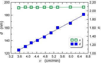
The relations of the final thickness d and the refractive index n of titania layers on the withdrawal speed are shown in Fig. 1. After the coating process, all structures were annealed at a temperature of 500 C for 60 min. Full blue diamond markers correspond to the experimental characteristics d = d(v), whereas empty green diamond markers correspond to the experimental dependence n = n(v). Refractive indices and layer thicknesses were determined by monochromatic ellipsometry. Both experimental characteristics d = d(v) and n = n(v) were approximated by linear functions.
The authors’ previous work [20] shows that this approach to approximation of the experimental character-istics d(v) is appropriate in a wide range of v. Using (1), a good approximation is obtained in narrower ranges of v variability. Titania layers of thickness varying in the range from 125 to 180 nm were obtained, if v was varying in the range from 3.6 cm/min to 7 cm/min. For the presented batch of TiO2 layers, their refractive indices remain at the same level of ~ 2.1, regardless of the value of v. All layers were crack-free and perfectly transparent.
Exemplary images of TiO2 layers deposited on fused silica glass substrates are shown in Fig. 2. In both cases, a uniform colour of the layer is visible on a wide area, which proves their optical homogeneity. Edge effects prevent a uniform film thickness over the full aperture of the substrate. One can observe stronger inhomogeneities in the area of substrates upper edges. They are the result of the detachment of a drop of sol when the substrate loses contact with the sol-free surface.

Fig. 3 shows the XRD spectra of TiO2 layers annealed in the air atmosphere at temperatures in the range from 200 °C to 700 °C for 60 min. It can be seen that TiO2 layers annealed at a temperature below 350 °C have an amorphous structure, increasing the annealing temperature results in the crystallization of TiO2. The broad peak at 23° can be observed in all spectra corresponding to amorphous SiO2 (fused silica) which is used as the substrate. The XRD spectra of TiO2 layers annealed at temperatures equal to or higher than 400 °C show additional peaks for 2θ equal to 25.44°, 37.94°, 48.36°, and 54.24°, which corresponds to the planes of anatase characterised by Miller indices (1 0 1), (0 0 4), (2 0 0), and (1 0 5), respectively [50, 51].

All diffraction peaks are well assigned to the anatase phase of TiO2. They are marked with asterisk characters.
The XRD pattern is matching the reference pattern JCPDS 21-1272 of TiO2. The peaks characterised by 2θ values equal to 25.44° and 48.36° confirm the presence of anatase. The characteristics showing the effect of the annealing temperature on the value of the nanocrystals diameter D is shown in Fig. 4. The latter was calculated using the Scherrer formula (2). As it can be observed, D increases if the annealing temperature increases up to 450 C. Above that temperature, the diameter of the anatase nanocrystals is no longer increasing.

The Raman spectra of TiO2 layers annealed at different temperatures are shown in Fig. 5. They are in the range from 100 to 1000 cm-1. Titanium oxide can exist in three main polymorphs such as tetragonal anatase, tetragonal rutile, and orthorhombic brookite [52]. The rutile phase is the most stable structure of TiO2, whereas the anatase phase to rutile phase transitions occurs above 600 C in the air atmosphere. Also, no rutile-derived peak was observed. The Raman spectra of TiO2 layers annealed above 500 C show symmetric modes of vibration of tetragonal anatase phase identified at 142 cm-1 (Eg); 195 cm-1 (Eg); 394 cm-1 (B1g); 515 cm-1 (A1g) and 638 cm-1. The symmetric stretching vibration, symmetric bending vibration, and anti-symmetric bending vibration of O-Ti-O are associated with the Eg, B1g, and A1g Raman modes. The intensity of the Raman vibration modes depends on the crystallinity of the titanium oxide. Their intensity depends on the annealing parameters, i.e., temperature, pressure, and presence of inert gas. The most substantial peak at 142 cm-1 appears due to an external symmetric vibration confirming the formation of a long-range order in the anatase phase [53–55]. The absence of anatase and rutile peaks indicates amorphousness of the TiO2 layers annealed below 350 C. It can be seen from the Raman spectra that the transformation from amorphous to anatase takes place at temperatures ranging from 300 °C to 350 °C.

The surface morphology of TiO2 layers deposited on soda-lime glass substrates was studied using AFM and SEM. SEM images of the surface of selected TiO2 layers annealed at different temperatures are shown in Fig. 6. The granular character of the layers is visible. The grains are randomly oriented and their size increases with the heating temperature. For the highest annealing temperature, the diameter of these grains is several tens of nanometres.

AFM images of the selected TiO2 layers are shown in Fig. 7. These results are consistent with those obtained by SEM. The grains diameter increases as the annealing temperature increases, leading to the increase in the RMS surface roughness (σRMS) as illustrated in Fig. 8. As expected, the smoothest layer is annealed at 300 C (σRMS = 0.25 nm). It has an amorphous structure (Figs. 3–5).

The characteristics of surface roughness as a function of the annealing temperature is presented in Fig. 8. The effect of the TiO2 layers annealing temperature on their final thicknesses d and refractive indices n is shown in Fig. 9. Full diamond markers present measured values of the thickness and empty diamond markers present measured values of the refractive index. As it can be seen, the thickness decreases monotonically as the annealing temperature increases.

The increase in annealing temperature from 150 C to 700 C results in a four-fold reduction of the titania layers thickness. On the characteristics of the refractive index, there is a narrow range of temperatures, starting at 350 C, where n decreases. The green, vertical, dashed line marks the centre of that range. This is probably the effect of the phase transition from the amorphous structure to the polycrystalline structure which is accompanied by the evaporation of organic compound residues. In the first range of the n(T) characteristics, the increase in n results from the collapse of the material structure. In the aforementioned narrow range, the evaporation of organic compounds results in the decrease of n, whereas in the third range n (T > 400 C), the increase in the refractive index is the result of further collapse of the TiO2 material structure and its crystallization. Red circle markers in Fig. 9 present the experimental dependence of the TiO2 layers porosity P on the annealing temperature. Porosity was calculated using (9) under the assumption that nd = 2.52 (anatase, λ = 632.8 nm). The characteristics of porosity is limited to the range of annealing temperatures equal to or higher than 400 C. That is because, for smaller temperatures, organic compounds of unknown concentration are present in the layers structure. As can be seen, porosity decreases from 17% to 8% if the annealing temperature increases from 400 °C to 700 C.

Spectrophotometry studies were carried out to determine the optical homogeneity of the fabricated TiO2 layers and to determine the positions of absorption edges and widths of the optical band gaps. Transmission spectra of selected TiO2 layers annealed at different temperatures are shown in Fig. 10. They were recorded in the UV-Vis-NIR spectral range. The grey line shows the transmission of the fused silica substrate. Interference maxima and minima are visible in these characteristics. For wavelengths below 350 nm, there is a sharp drop in transmission resulting from the presence of absorbing edges in this spectral range. For wavelengths above 500 nm, the interference maxima lie on the transmission characteristics of the substrate, which indicates the optical homogeneity of the layers. With the increase of the annealing temperature, depth of the interference minima increases, which is the result of the increase in the layers refractive index (Fig. 10).

TiO2 layers optical energy band gap widths and the absorption coefficients α were determined from trans-mission spectra. The widths of band gaps of TiO2 layers annealed at different temperatures were calculated by plotting the Tauc equation, which shows the relationship between the absorption coefficient and photon energy [56]
\( (\alpha h v)^{1 / \gamma}=A\left(h v-E_g\right) \) (10)
Herein, A is the absorption constant which does not depend on photon energy (hν), Eg is the band gap width, 𝜈 is the frequency of the incident radiation, and h is Planck constant. The γ factor depends on the nature of the electron transition and is equal to 1/2 or 2 for the direct and indirect transition band gaps, respectively.
Fig. 11 shows the Tauc plots of (αhν)¹/² as a function of (hν) for indirect and direct optical transitions in the TiO2 layers of thickness d = 153 nm. The layers were deposited on fused silica substrates and annealed at temperatures of 250 °C and 500 °C, respectively. The optical band gaps were calculated by extrapolating the linear part of the experimental curves towards lower energies. The point at which the extrapolated line crosses the horizontal axis determines the value of the optical band gap.

Charac- teristics of optical energy band gap widths as a function of the annealing temperature were determined by applying this procedure to transmission characteristics of titania layers annealed at different temperatures. They are shown in Fig. 12, for both indirect and direct optical transitions. For all films, energy blue shift vs. bulk anatase (Eg ind = 3.2 eV) can be observed. This phenomenon is called the quantum size effect [32]. Moreover, for presented TiO2 layers, a decrease in the optical band gaps with increasing annealing temperature can be also observed. This effect is associated with the increase in the size of the TiO2 nanocrystals with increasing annealing temperature (Fig. 4). Vasantkumar et al. [57] postulated that the observed decrease in the band gap energy with the increase in annealing temperature results from the reduction of interatomic spacing (amorphous→crystalline).

A strong influence of the annealing temperature on the optical band gaps is observed for temperatures lower than 400 °C. The increased dispersion of Eg_ind measurement points in this temperature range is probably the result of the instability of the layer parameters caused by the presence of organic residues in them. Above the temperature of 400 °C, a weak effect of the annealing temperature on the optical band gaps is observed. Such a significant dispersion of Eg_ind measurement points is not observed in this temperature range. The average width of the optical band gap corresponding to the indirect transitions for layers annealed at temperatures above 400 °C is 3.36 eV.
The registered dispersion characteristics of the ellipsometric angles Ψ and Δ, recorded for the TiO2 layers deposited on silicon substrates and annealed at 500° C, are shown in Fig. 13. Measurements were made for four different illumination angles of the examined structure (60°, 65°, 70°, and 75°). Experimental characteristics recorded for individual angles of illumination of the tested sample are plotted by continuous coloured lines. The calculated characteristics, corresponding to the perfect fit with the experimental characteristics are plotted using dashed dot lines. Excellent agreement of the modelled and measured characteristics can be observed for any angle of illumination. Chromatic dispersion characteristics of the refractive index n (λ) and the extinction coefficient κ (λ) were calculated using the Tauc-Lorentz dispersion model.

Chromatic dispersion characteristics of the refractive index n(λ) and extinction coefficient κ (λ) for selected annealing temperatures are shown in Fig. 14(a) and Fig. 14(b), respectively. A normal dependence of the refrac-tive index on the wavelength for λ > 300 nm can be observed.

Anomalous dispersion for wavelengths less than 300 nm results from the presence of absorption edges in this wavelength range where the extinction coefficient increases (Fig. 10). Over the full range of the wavelength spectrum, both the refractive index n and the extinction coefficient κ increase with the increase in annealing temperature. The refractive index increase as a result of material densification during the annealing process. The evaporation effect of organic residues plays an additional role at lower temperatures. The increase in the extinction coefficient, associated with the increase in temperature, is mainly the result of the increase in the size of nanocrystals and the shift of the absorption edge toward higher wavelengths.
Conclusions
Homogeneous, crack-free titania layers, the thickness of which exceeds 100 nm were fabricated using the combination of the sol-gel method and dip-coating technique. The titania (IV) ethoxide was used as the precursor, whereas reactions of hydrolysis and condensation were catalysed with hydrochloric acid. The effect of annealing temperature on titania layer structure, surface morphology, and optical properties was examined. The investigations carried out using XRD and Raman spectroscopy have shown that TiO2 layers annealed at temperatures below 300 °C are amorphous. Above this temperature, they become polycrystalline, but they comprise only anatase nanocrystals. The size of the nanocrystals diameter increases with an increase in the annealing temperature up to 450 °C. The further increase in tempera- ture does not increase the anatase nanocrystal diameter.
Investigations on surface morphology carried out using the AFM method have shown that the RMS surface roughness is less than 1 nm if the annealing temperature does not exceed 500 °C. The roughness increases up to 3 nm for higher annealing temperatures. The spectro- photometric investigations have shown that titania layers are optically uniform. The effect of annealing temperature on the optical band gaps width was carried out by analysis of the absorption edge using the Tauc method. The ellipsometric studies allowed to determine the effect of annealing temperature on the thickness and refractive index of TiO2 layers. The porosity of TiO2 layers changes from 18% down to 8% for the increase of annealing temperature from 400 °C to 700 °C. In this range of temperatures, the widths of optical band gaps become stabilized at the level of ~ 3.36 eV for indirect transitions and ~ 3.69 eV for direct transitions. Chromatic dispersion characteristics of the refractive index and extinction coefficient were determined for selected values of annealing temperature using spectroscopic ellipsometry. Elaborated titania layers are suitable for applications in multilayer antireflective structures on solar glasses.
Authors’ statement
M.Z.: conceptualization, investigation, formal analysis, writing – original draft, writing – review & editing, visuali-zation, funding acquisition; C.T.: investigation, software, formal analysis, writing – original draft, writing – review & editing, visualization; E.G.: investigation, formal analysis, validation; K.W.: investigation, formal analysis, validation, writing – review & editing; J.N.: investigation, formal analysis, validation; D.D.: investigation, formal analysis, validation, supervision; B.S.: investigation, formal analysis, validation; P.S.: investigation, formal analysis, validation; W.P.: investigation, formal analysis, validation; R.R.: formal analysis, resources, writing – review & editing; P.K.: conceptualization, software, formal analysis, writing – original draft, writing – review & editing, visualization, supervision.
Acknowledgements
This research was funded as part of the pro-quality grant for ground-breaking research (No. 32/014/SDU/10-21-01) of the Excellence Initiative – Research University program implemented at the Silesian University of Technology (2021). Also, this research was partially financially supported within a scope of the TEAM-NET project: “Hybrid sensor platforms of integrated photonic systems based on ceramic and polymer materials (HYPHa)” from the Foundation for Polish Science. Project no.: POIR.04.04.00-00-14D6 /18-00.
References
-
Miao, L. et al. Microstructure and bactericidal ability of photo- catalitic TiO2 thin films prepared by rf helicon magnetron sputtering. Appl. Surf. Sci. 238, 125–131 (2004). https://doi.org/10.1016/j.apsusc.2004.05.193
-
Liu, W., Zou, B., Zhao, J. & Cui, H. Optimizing sol-gel infiltration for the fabrication of high-quality titania inverse opal and its photocatalytic activity. Thin Solid Films 518, 4923–4927(2010). https://doi.org/10.1016/j.tsf.2010.02.043
-
Guo, Q., Zhou, C., Ma, Z. & Yang, X. Fundamentals of TiO2 photocatalysis: concepts, mechanisms, and challenges. Adv. Mater. 31, 1901997 (2019). https://doi.org/10.1002/adma.201901997
-
Al-Mamun, M. R., Kader, S., Islam, M. S. & Khan, M. Z. H. Photocatalytic activity improvement and application of UV-TiO2 photocatalysis in textile waste water treatment: A review.J. Environ. Chem. Eng. 7, 103248 (2019). https://doi.org/10.1016/j.jece.2019.103248
-
Lukong, V. T., Ukoba, K. & Jen, T.-Ch. Review of self-cleaning TiO2 thin films deposited with spin coating. Int. J. Adv. Manuf. Technol. 122, 3525–3546 (2022).https://doi.org/10.1007/s00170-022-10043-3
-
Zhao, W. et al. Sol-gel synthesis of TiO2-SiO2 hybrid films with tunable refractive index for broadband antireflective coatings covering the visible range. J. Sol-Gel. Sci. Technol. 107, 105–121 (2023). https://doi.org/10.1007/s10971-021-05719-3
-
Skolik, M., Domanowska, A., Karasiński, P., Gondek, E. & Michalewicz, A. Double layer sol-gel derived antireflective coatings on silicon – Design, optical and Auger electron spectroscopy characterization. Mater. Lett. 251, 210–213 (2019). https://doi.org/10.1016/j.matlet.2019.05.071
-
Gondek, E. & Karasiński, P. One-dimensional photonic crystals as selective back reflectors. Opt. Laser Technol. 48, 438–446 (2013). https://doi.org/10.1016/j.optlastec.2012.11.012
-
Dinh, N. N., Oanh, N. Th. T., Long, P. D., Bernard M. C. & Hugot- Le Goff, A. Electrochromic properties of TiO2 anatase thin films prepared by a dipping sol-gel method. Thin Solid Films 423, 70–76 (2003). https://doi.org/10.1016/S0040-6090(02)00948-3
-
Honda, T. et al. Optically pumped ZnSe-based vertical cavity surface emitter with SiO2/TiO2 multilayer reflector. J. Appl. Phys. 78, 4784–4786 (1995). https://doi.org/10.1063/1.359758
-
Hu, W., Yang, S. & Yang, S. Surface modification of TiO2 for perovskite solar cells. Trends Chem. 2, 148–162 (2020). https://doi.org/10.1016/j.trechm.2019.11.002
-
Alturki, A. A. et al. Polymeric solar cell with 18.06% efficiency based on poly(para-nitroaniline)/TiO2 composites. Opt. Mater. 136, 113502 (2023). https://doi.org/10.1016/j.optmat.2023.113502
-
Devadiga, D., Selvakumar, M., Shetty P. & Santosh, M. S., Dye- sensitized solar cell for indoor applications: A mini-review, J. Electron. Mater. 50, 3187–3206 (2021). https://doi.org/10.1007/s11664-021-08854-3
-
Adewinbi, S. A. Preparation and characterization of TiO2 thin film electrode for optoelectronic and energy storage potentials: effects of Co incorporation. Chem. Phys. Lett. 779, 138854 (2021). https://doi.org/10.1016/j.cplett.2021.138854
-
Zaban, A., Meier, A. & Gregg, B. A. Electric potential distribution and short-range screening in nanoporous TiO2 electrodes. J. Phys.Chem. B 101, 7985–7990 (1997). https://doi.org/10.1021/jp971857u
-
Rzaij, J. M. & Abass, A. M. Review on: TiO2 thin film as a metal oxide gas sensor. J. Chem. Rev. 2, 114–121 (2020). https://doi.org/10.33945/SAMI/JCR.2020.2.4
-
Tian, X. et al. Gas sensors based on TiO2 nanostructured materials for the detection of hazardous gases: A review. Nano Mater. Sci. 3, 390–403 (2021). https://doi.org/10.1016/j.nanoms.2021.05.011
-
D’Agostino, M. et al. Antibacterial titanium dioxide coatings for CoCrMo orthopaedic implants. Appl. Surf. Sci. 609, 155300 (2023). https://doi.org/10.1016/j.apsusc.2022.155300
-
Catauro, M., Dal Poggetto, G., Risoluti, R. & Vecchio Ciprioti, S. Thermal, chemical and antimicrobial characterization of bioactive titania synthesized by sol-gel method. J. Therm. Anal. 142, 1767– 1774 (2020). https://doi.org/10.1007/s10973-020-10264-2
-
Karasiński, P. et al. Sol-gel derived silica-titania waveguide films for applications in evanescent wave sensors–comprehensive study. Materials 15, 7641 (2022). https:// doi.org/10.3390/ma15217641
-
Karasiński, P. et al. Homogeneity of sol-gel derived silica-titania waveguide films – spectroscopic and AFM studies. Opt. Laser Technol. 121, 105840 (2020). https://doi.org/10.1016/j.optlastec.2019.105840
-
Touam, T. et al. Low loss sol-gel TiO2 thin films for waveguiding aplications. Coatings 3, 49–58 (2013). https://doi.org/10.3390/coatings3010049
-
Bradley, J. D. B. et al. Submicrometer-wide amorphous and polycrystalline anatase TiO2 waveguides for microphotonic devices. Opt. Express 20, 23821–23831 (2012).https://doi.org/10.1364/OE.20.023821
-
Aroutiounian, V., Arakelyan, V., Galstyan, V., Martirosyan, K. & Soukiassian, P. Hydrogen sensor made of porous silicon and covered by TiO2-x or ZnO <Al> thin film. IEEE Sens. J. 9, 9–12 (2009). https://doi.org/10.1109/JSEN.2008.2008406
-
Kot, A., Radecka, M. & Zakrzewska, K. Influence of Er and Yb on photoelectrochemical performence of TiO2 thin film. Appl. Surf. Sci. 608, 155127 (2023). https://doi.org/10.1016/j.apsusc.2022.155127
-
Tao, R. H. et al. Pulsed laser deposition of titania on rutile nanorod arrays. Thin Solid Films 518, 4191–4196 (2010). https://doi.org/10.1016/j.tsf.2009.12.002
-
Nakaruk, A., Ragazzon, D. & Sorrell, C. C. Anatase-rutile trans- formation through high-temperature annealing of titania films produced by ultrasonic spray pyrolysis. Thin Solid Films 518, 3735– 3742 (2010). https://doi.org/10.1016/j.tsf.2009.10.109
-
Zhang, W. Z., Zhang, T., Yin, W. & Cao, G. Relationship between photocatalytic activity and structure of TiO2 thin film. Chinese J. Chem. Phys. 20, 95–98 (2007).https://doi.org/10.1360/cjcp2007.20(1).95.4
-
Babelon, P. et al. SEM and XPS studies of titanium dioxide thin films grown by MOCVD. Thin Solid Films 322, 63–67 (1998). https://doi.org/10.1016/S0040-6090(97)00958-9
-
Saha, D. et al. Spectroscopic ellipsometry characterization of amorphous andcrystalline TiO2 thin films grown by atomic layer deposition at different temperatures. Appl. Surf. Sci. 315, 116–123 (2014). https://doi.org/10.1016/j.apsusc.2014.07.098
-
Szindler, M., Szindler, M. M., Orwat, J. & Kulesza-Matlak, G. The Al2O3/TiO2 double antireflection coating deposited by ALD method. Opto-Electron. Rev. 30, e141952 (2022). https://doi.org/10.24425/opelre.2022.141952
-
Gondek, E., Karasiński, P. & Drewniak S. Nano-quantum size effect in sol–gel derived mesoporous titania layers deposited on soda-lime glass substrate. Physica E Low Dimens. Syst. Nanostruct. 62, 128– 135 (2014). https://doi.org/10.1016/j.physe.2014.04.018
-
Brinker, C. J. & Scherer, G. W. Sol-Gel Science: The Physics and Chemistry of Sol-Gel Processing. (Academic Press, San Diego, 1990).
-
Duta, M. et al. Structural and electrical properties of Nb doped TiO2 films prepared by the sol-gel layer-by-layer technique. Mater. Res. Bull. 74, 15–20 (2016). https://doi.org/10.1016/j.materresbull.2015.10.009
-
Kim, D. J., Hahn, S. H., Oh, S. H. & Kim, E. J. Influence of calcination temperature on structural and optical properties of TiO2 thin films prepared by sol-gel dip coating. Mater. Lett. 57, 355–360 (2002). https://doi.org/10.1016/S0167-577X(02)00790-5
-
Mechiakh, R. et al. TiO2 thin films prepared by sol-gel method for waveguiding applications: Correlation between the structural and optical properties. Opt. Mater. 30, 645–651 (2007). https://doi.org/10.1016/j.optmat.2007.02.047
-
Mechiakh, R., Ben Sedrine, N., Ben Naceur, J. & Chtourou R. Elaboration and characterization of nanocrystalline TiO2 thin films prepared by sol-dip-coating. Surf. Coat. Technol, 206, 243–249 (2011). https://doi.org/10.1016/j.surfcoat.2011.06.053
-
Ye, L. et al. Sol-gel preparation of SiO2/TiO2/SiO2–TiO2 broad- band antireflective coating for solar cell cover glass. Sol. Energy Mater. Sol. Cells. 111, 160–164 (2013). https://doi.org/10.1016/j.solmat.2012.12.037
-
Karasiński, P., Tyszkiewicz, C., Rogoziński, R., Jaglarz, J. & Mazur,J. Optical rib waveguides based on sol-gel derived silica-titania films. Thin Solid Films, 519, 5544–5551 (2011). https://doi.org/10.1016/j.tsf.2011.02.064
-
Klein, L. C. Sol-Gel Optics: Procesing and Applications. (Kluwer Academic Publishers, Boston, 1994).
-
Strawbridge, I. & James, P. F. The factors affecting the thickness of sol-gel derived silica coatings prepared by dipping. J. Non-Cryst. 86, 381–393 (1986). https://doi.org/10.1016/0022-3093(86)90026-8
-
Azzam, R. M. A. & Bashara, N. M. Ellipsometry and Polarized Light. (North-Holland Personal Library, 1999). Available online: https://www.amazon.com/Ellipsometry-Polarized-North-Holland-Personal-Library/dp/0444870164 (accessed on 14 May 2021).
-
Bendavid, A., Martin, P. J., Jamting, Å. & Takikawa, H., Structural and optical properties of titanium oxide thin films deposited by filtered arc deposition. Thin Solid Films 355-356, 6–11 (1999). https://doi.org/10.1016/S0040-6090(99)00436-8
-
Postava, K., Aoyama, M., Yamaguchi, T. & Oda, H. Spectro- ellipsometric characterization of materials for multilayer coatings. Appl. Surf. Sci. 175–176, 276–280 (2001). https://doi.org/10.1016/S0169-4332(01)00163-5
-
Blanckenhagen, B., Tonova, D. & Ullmann, J. Application of the Tauc-Lorentz formulation to the interband absorption of optical coating materials. Appl. Opt. 41, 3137–3141 (2002). https://doi.org/10.1364/AO.41.003137
-
Blanco, E. et al. Insights into the annealing process of sol-gel TiO2 films leading to anatase development: The interrelationship between microstructure and optical properties. Appl. Surf. Sci. 439, 736–748 (2018). https://doi.org/10.1016/j.apsusc.2018.01.058
-
Jellison, G. E. & Modine, F. A. Erratum: Parameterization of the optical functions of amorphous materials in the interband region. Appl. Phys. Lett. 69, 2137 (1996). https://doi.org/10.1063/1.118155
-
Jellison, G.E. & Modine, F. A. Parameterization of the optical functions of amorphous materials in the interband region. Appl.Phys. Lett. 69, 371–373 (1996). https://doi.org/10.1063/1.118064
-
Jellison, G. et al. Characterization of thin-film amorphous semi- conductors using spectroscopic ellipsometry. Thin Solid Films 377– 378, 68–73 (2000). https://doi.org/10.1016/S0040-6090(00)01384-5
-
Hassanien, A. S. & Akl, A. A. Optical characterizations and refractive index dispersion parameters of annealed TiO2 thin films synthesized by RF-sputtering technique at different flow rates of the reactive oxygen gas. Physica B Condens. Matter. 576, 411718 (2020). https://doi.org/10.1016/j.physb.2019.411718
-
Mathews, N. R., Morales, E. R., Cortés-Jacome, M. A. & Toledo Antonio, J. A. TiO2 thin films – Influence of annealing temperature on structural, optical and photocatalytic properties. Sol. Energy 83, 1499–1508 (2009). https://doi.org/10.1016/j.solener.2009.04.008
-
Yan, J. et al. Understanding the effect of surface/bulk defects on the photocatalytic activity of TiO2: anatase versus rutile. Phys. Chem. Chem. Phys. 15, 10978–10988 (2013).https://doi.org/10.1039/c3cp50927c
-
Boda, M. A. & Shah, M. A. Fabrication mechanism of compact TiO2 nanotubes and their photo-electrochemical ability. Mater. Res.Express 4, 075908 (2017). https://doi.org/10.1088/2053-1591/aa7cd2
-
Ekoi, E. J., Gowen, A., Dorrepaal R. & Dowling, D. P. Characterisation of titanium oxide layers using Raman spectroscopy and optical profilometry: Influence of oxide properties. Results Phys. 12, 1574–1585 (2019). https://doi.org/10.1016/j.rinp.2019.01.054
-
Montagna, M. et al. Nucleation of titania nanocrystals in silica titania waveguides. J. Sol-Gel Sci. Technol. 26, 241–244 (2003). https://doi.org/10.1023/A:1020755200573
-
Tauc, J. Optical Properties of Amorphous Semiconductors. in Amorphous and Liquid Semiconductors (ed. Tauc, J.) 159–220 (Springer, 1974). https://doi.org/10.1007/978-1-4615-8705-7_4
-
Vasantkumar, C. V. R. & Mansingh, A. Properties of RF Sputtered Tetragonal and Hexagonal Barium Titanate Films. in 7th IEEE International Symposium on Application of Ferroelectrics (ISAF) 713–716 (IEEE, New York, 1990).