Characterisation of a graphene/NPB structure with Re2O7 as an interfacial layer for OLED application
- Department of Solid State Physics (member of National Photovoltaic Laboratory, Poland), Faculty of Physics and Applied Informatics, University of Lodz, ul. Pomorska 149/153, 90-236 Łódź, Poland/li>
- Department of Physics, University of Kalyani, Kalyani-741235, Nadia, West Bengal, India
- Department of Molecular Physics (member of National Photovoltaic Laboratory, Poland), Lodz University of Technology, ul. Żeromskiego 116, 90-924 Łódź, Poland
Article Info
Received 15 Jun. 2023
Received in revised form 09 Oct. 2023
Accepted 16 Oct. 2023
Available on-line 23 Nov. 2023
Keywords: Graphene; rhenium oxide; NPB; anode.
Abstract
A graphene/NPB structure with Re2O7 as an interfacial layer in the context of its potential use in the design of an organic light-emitting diode (OLED) is investigated. The X-ray photoelectron spectroscopy (XPS) study shows the formation of the Re2O7 phase on a monolayer graphene on quartz during thermal deposition in ultra-high vacuum (UHV). The ultraviolet photoelectron spectroscopy (UPS) study shows an enhancement of the work function of the graphene heterostructure after deposition of the Re2O7 layer up to 5.4 eV. The hole injection barrier between the Re2O7/graphene heterostructure and the N-bis-(1- naphthyl)-N,N-diphenyl-(1,1-biphenyl)-4,4-diamine (NPB) layer was estimated to be 0.35 eV, which is very promising for a good OLED performance.
Introduction
It is well known that graphene, being a two-dimensional (2D) carbon allotrope, has unique electrical, optical, thermal, and mechanical properties [1]. Therefore, due to its high electrical conductivity, transparency in the visible range of electromagnetic radiation, and flexibility, graphene can be considered an electrode in constructing an organic light-emitting diode (OLED). A new type of graphene electrode may shortly replace the standard indium tin oxide (ITO) electrode in the construction of the OLED [2]. In addition, it should be emphasized that the flexibility of graphene makes it possible to consider the use of a graphene electrode in flexible and rollable displays [3]. The construction of a flexible OLED display based on an anode made of ITO is very difficult due to the fragility of ITO. However, pristine and undoped graphene is not suitable as an electrode because the work function of graphene is not matched to the energy levels of the organic layers used for OLED fabrication. Graphene, depending on the number of layers, defects, disorder, and substrate, has a work function in the range of 3.9 – 4.8 eV [4–6]. To effectively operate as an anode in optoelectronic devices, the work function of the graphene electrode should be significantly increased up to 5.2 – 5.4 eV. The work function must be at a sufficiently high level to minimize the potential barrier in the process of injecting charge carriers, i.e., holes from the graphene anode into organic layers [5].
Various methods of graphene production exist, based on both physical processes (mechanical exfoliation of graphite, sublimation of Si atoms from the SiC surface, epitaxial growth) and chemical processes [chemical vapour deposition (CVD) on metallic catalyst substrates, reduction of graphene oxide] [7]. This opens wide possibilities for the industrial production of graphene and its optimization in the context of OLED devices. However, in each of these cases, the work function of the graphene electrode must be additionally modified.
Adjusting the work function of graphene to the energy levels of organic layers in an OLED device can be achieved by several methods including doping aromatic molecules, surface functionalization, ultraviolet irradiation, electro-static gating [8], and depositing transition metal oxides (TMO) [9]. The authors’ research focuses on the modification of graphene work function with TMO such as MoO3, Re2O7, and TiO2 [4-11,15]. For example, to gain a better insight into the growth of MoO3 on graphene, the authors have carried out fundamental research related to the growth of a 2D MoO3 with a monolayer thickness on a highly oriented pyrolytic graphite (HOPG) [10–12]. It was revealed that the crystallinity of 2D materials is crucial for an efficient work function modification of HOPG. Intriguingly, the crystalline MoO3 monolayer with thick-nesses as low as 0.7 nm increases HOPG work function up to 6.4 eV [11]. Thus, graphene work function can be enhanced by covering it with a 2D crystalline layer of TMO such as MoO3 [10, 11]. Additionally, it was shown that the work function of high-quality graphene grown on SiC(0001) can be successfully increased to 4.95 eV by covering it with thermally evaporated Re2O7 which is relevant in the context of optoelectronic applications [13].
In authors’ previous paper [4], it was shown that the work function of a monolayer graphene on quartz can be modified with rhenium oxide and such heterostructure meets the basic requirements for use as a transparent anode in OLED applications [4]. The following is research on modification of the work function of a monolayer graphene on quartz with the incremental deposition of rhenium oxide. Additionally, the authors go a step forward and discuss the structure formation between graphene on quartz and a prototypical “hole transport layer” N,N-bis-(1-naphthyl)-N,N-diphenyl-(1,1-biphenyl)-4,4-diamine (NPB) using rhenium oxide as an interfacial layer. NPB is an organic material used widely as a hole transport layer in OLED with ITO as an electrode [16–18]. It is well known that the electroluminescence stability of OLED based on the ITO anode is strongly affected by the presence of the NPB hole transport layer and its thickness [19].
Experimental methods
Commercially available monolayer graphene on quartz (transparency: > 97%, coverage: > 98%, sheet resistance: 360 ± 30 Ω/, MSE Supplies LLC) was used. Dirhenium heptoxide powder (Re2O7, purity: 99.9%, Aldrich) and NPD (purity: > 99.0%, Ossila) were evaporated from crucibles in a thermal deposition process in ultra-high vacuum (UHV). The working pressure was ~ 6 × 10⁻⁹ mbar during Re2O7 deposition. A quartz-crystal microbalance was used to estimate the thickness of Re2O7 and NPB layers.
X-ray photoelectron spectroscopy (XPS) study was carried out with a non-monochromatic X-ray radiation of 1253.64 eV (Mg Kα) from a DAR 400 source lamp (Omicron) operating with a Phoibos 150 hemispherical electron energy analyser (SPECS) combined with a 2D CCD detector. The Shirley method was used for background subtraction.
The ultraviolet photoelectron spectroscopy (UPS) study was carried out with a HIS-13 UV lamp (Omicron) using the HeIa line with an energy of 21.23 eV and a Phoibos 150 analyser. The UPS spectra were calibrated using the Fermi level of a pure Au(111) surface. A negative potential of 3.1 V was applied to the sample to determine the back- scattered electron emission edge. The XPS and UPS spectra were analysed with the CasaXPS software package [20].
An atomic force microscope (AFM) study was carried out with the Ntegra Aura (NT-MDT) working in semi- contact mode under ambient air conditions. AFM imageswere processed using Gwyddion.
Results and discussion
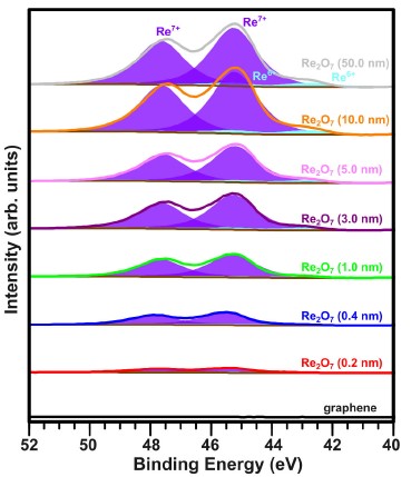
The authors first performed an XPS study to determine the stoichiometry of rhenium oxide layers formed on graphene on quartz after thermal deposition of Re2O7 from powder in UHV. Figure 1 shows the XPS spectra of the Re 4f core level of pristine graphene and graphene covered with the incremental layers of rhenium oxide grown using the step-by-step deposition method. The authors started with a nominal thickness of 0.2 nm, up to 50 nm. In the deconvolution process of the Re 4f spectra, a characteristic 4f7/2–4f5/2 doublet related to the single oxidation state, with an energy splitting of 2.4 eV and relative integrated peak areas of 4:3 (resulting from the spin-orbit coupling), was fixed. Peak fitting was performed using mixed Gaussian/Lorentzian line shapes [GL(75)] with a full width at half maximum (FWHM) ranging from 1.7 to 1.85 eV. The XPS spectra deconvolution shows the presence of 4f7/2and 4f5/2 spin-orbit doublet peaks at binding energies of about 45.4 and 47.8 eV, respectively. Thus, it was concluded that the oxide layers formed on graphene on quartz are composed mainly of Re7+ oxidation state exhibiting the formation of Re2O7 phase, which is thermo- dynamically the most stable phase of rhenium oxide. This is in good agreement with reference works from the literature [21, 22] and authors previous reports [4, 13].

Additionally, the presence of a very small amount of Re6+ with 4f7/2 and 4f5/2 spin-orbit doublet peaks was identified at binding energies of about 42.9 and 45.3 eV respectively, indicating the formation of a ReO3 phase.
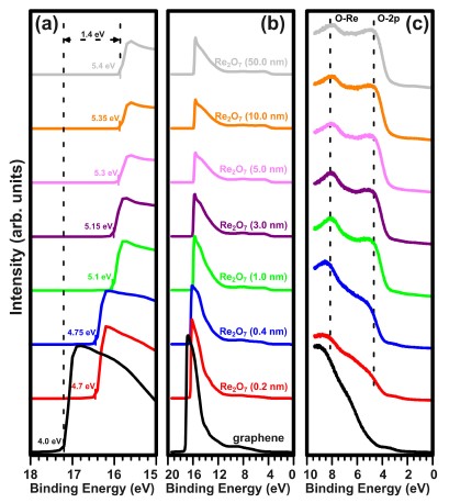
Figure 2 shows the UPS spectra of (a) the secondary electron cut-off region, (b) the full range, and (c) the valence band (VB) region of pristine graphene on quartz and Re2O7/graphene heterostructure with incremental rhenium oxide thicknesses. The work function of pristine graphene, derived from the secondary electron cut-off, was estimated to be 4.0 eV [see the black curve in Fig. 2(a)] [23]. As the rhenium oxide thickness increases, the secondary electron cut-off shifts towards lower binding energies. This demon-strates an increase in the work function of Re2O7/graphene heterostructure with increasing thicknesses of rhenium oxide. Even very low thicknesses of Re2O7 increase the work function significantly: the work function of graphene, covered with only 0.2 nm of Re2O7 is estimated to be 4.7 eV. The deposition of a 5 nm thick layer leads to a large increase in the work function (5.3 eV), near the saturation value.

Further deposition of the Re2O7 does not contribute to the significant increase of the work function of the heterostructure. Upon the deposition of a 50 nm thick layer of Re2O7, the work function of heterostructure is estimated to be 5.4 eV. Please note that above the coverage corre-sponding to 1 nm, no significant change in the shape of the measured secondary electron cut-off edges is observed. This suggests that above 1 nm the authors are dealing with a continuous or nearly continuous oxide layer and not an island manner as was the case with MoO3 [11]. This achieved values of work function for heterostructure is high enough to inject holes to the hole transport layer made from organic semiconductors with high HOMO levels such as NPB, thus it can be considered as an effective anode in OLED. Note that the work function of Re2O7 deposited on graphene is much lower than that of rhenium foil after oxidation of 7.1 eV [24]. It is well known that the change in work function can be ascribed to the formation of surface dipole and to interfacial band bending [25]. However, owing to the peculiar electronic structure of a monolayer graphene, the work function increase is associated here with the formation of surface negative dipole, which arises from electron transfer from Re2O7 to graphene. The same effect is observed for the MoO3/graphene interface [25]. Additionally, the peaks at about 5 and 8 eV are attributed to O 2p-derived states and to a mixture of oxygen/rhenium states, respectively [26]. Gap states in the band gap of Re2O7 were not observed.
To further investigate the Re2O7/graphene heterostruc-ture in the context of applications to OLED design, a typical hole transport layer, NPB, was deposited.
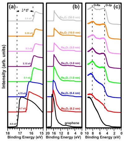
Figure 3 shows the UPS spectra of (a) the secondary electron cut-off region, (b) the full range, and (c) the VB region of Re2O7/graphene heterostructure with an oxide thickness of 1.0 nm and after deposition of the NPB hole transport layer, with variable thickness (from 0.2 nm to 50.0 nm) using the step-by-step deposition method. As indicated by the data, the secondary electron cut-off position shifts towards higher binding energies with increasing NPB thickness. After a deposition of a 50 nm layer of NPB, the secondary cut-off shift is estimated to be 1.4 eV. The hole injection barrier, estimated as the energy difference between the HOMO edge and the Fermi level, is very small (0.35 eV for a 0.5 nm thickness of NPB), and thus very promising in terms of OLED devices performance.

To evaluate the surface morphology of the NPB hole transport layer deposited on the Re2O7/graphene hetero-structure, an AFM study was carried out. Figure 4 shows the topographic image of the Re2O7/graphene heterostructure with an oxide thickness of 1.0 nm covered with a 50 nm layer of NPB. The authors focus on an NPB layer with a thickness of 50 nm as it is commonly used in OLED quality benchmarking [18]. The AFM image suggests that NPB forms a uniform and flat layer on the Re2O7/graphene heterostructure. The root-mean-square (RMS) roughness of the heterostructure is estimated to be 1.2 nm. The bright protrusion can be ascribed to poly(methyl methacrylate) (PMMA) residue remaining after graphene transfer from the copper foil onto quartz. The AFM investigation demonstrates that the surface roughness of a 50 nm thick NPB layer formed on the Re2O7/graphene heterostructure is sufficiently low for the deposition of a subsequent layer, i.e., the emissive layer in OLED device structures [18].

Conclusions
The authors investigated the interaction between rhenium oxide thin films of various thicknesses on a monolayer graphene on quartz, using XPS and UPS techniques. XPS study shows the formation of the Re2O7 phase on graphene on quartz during thermal deposition in UHV. UPS study shows that the Re2O7 layer can successfully enhance the work function of graphene. The deposition of Re2O7 on graphene on quartz increases work function up to 5.4 eV resulting from electron transfer from graphene to Re2O7 with a higher electron affinity. This value of heterostructure work function is high enough to efficiently inject holes into the hole transport layer with high HOMO levels such as NPB, and thus Re2O7/graphene can be considered as an effective transparent anode in OLED devices. To further verify the potential integrability of Re2O7 into OLED structures, an NPB hole transport layer of various thicknesses was then deposited onto the Re2O7/graphene heterostructure. UPS study shows that the hole injection barrier between the NPB layer and the Re2O7/graphene heterostructure is only 0.35 eV, which guarantees good performance of OLED devices based on this heterostructure. Finally, the AFM study evidences a uniform and flat morphology of the NPB layer on the Re2O7/graphene heterostructure.
Authors’ statement
Research concept and design, P.K., P.D., and M.R.; collection of data, P.K., M.P., M.R., P.D., I.L., W.K., D.A.K., P.Kre., M.L.S., A.N., K.T., P.P., R.D., W.R., and S.S.; data analysis and interpretation, P.K., M.P., P.D., and M.R.; critical revision of the article, M.R., D.A.K., B.Ł., and P.J.K.; final approval of article, B.Ł. and P.J.K.
Acknowledgements
This work was financially supported by the National Science Centre (Poland) under grants 2016/21/B/ST5/00984 and 2020/37/B/ST5/03929.
References
-
Rao, C. N. R., Sood, A. K., Subrahmanyam, K. S. & Govindaraj, A. Graphene: The new two-dimensional nanomaterial. Angew. Chem. Int. Ed. 48, 7752–7777 (2009). https://doi.org/10.1002/anie.200901678
-
Weng, Z. et al. Wafer-scale graphene anodes replace indium tin oxide in organic light-emitting diodes. Adv. Opt. Mater. 10, 2101675 (2022). https://doi.org/10.1002/adom.202101675
-
Kwon, O. E. et al. A prototype active-matrix OLED using graphene anode for flexible display application. J. Inf. Disp. 21, 49–56 (2020). https://doi.org/10.1080/15980316.2019.1680452
-
Krukowski, P. et al. Graphene on quartz modified with rhenium oxide as a semitransparent electrode for organic electronics. Opto- Electron. Rev. 30, e141953 (2022). https://doi.org/10.24425/opelre.2022.141953
-
Naghdi, S., Sanchez-Arriaga, G. & Rhee, K. Y. Tuning the work function of graphene toward application as anode and cathode. J. Alloys Compd. 805, 1117–1134 (2019). https://doi.org/10.1016/j.jallcom.2019.07.187
-
Yoon, T., Wu, Q., Yun, D.-J., Kim, S. H. & Song, Y. J. Direct tuning of graphene work function via chemical vapor deposition control. Sci. Rep. 10, 9870 (2020). https://doi.org/10.1038/s41598-020-66893-y
-
Tan, R. K. L. et al. Graphene as a flexible electrode: review of fabrication approaches. J. Mater. Chem. A 5, 17777–17803 (2017). https://doi.org/10.1039/C7TA05759H
-
Yang, N. et al. Design and adjustment of the graphene work function via size, modification, defects, and doping: a first-principle theory study. Nanoscale Res. Lett. 12, 642 (2017). https://doi.org/10.1186/s11671-017-2375-3
-
Meyer, J. et al. Metal oxide induced charge transfer doping and band alignment of graphene electrodes for efficient organic light emitting diodes. Sci. Rep. 4, 5380 (2014). https://doi.org/10.1038/srep05380
-
Kowalczyk, D. A. et al. Local electronic structure of stable monolayers of α-MoO3−x grown on graphite substrate. 2D Mater. 8, 25005 (2020). https://doi.org/10.1088/2053-1583/abcf10
-
Kowalczyk, D. A. et al. Two-dimensional crystals as a buffer layer for high work function applications: the case of monolayer MoO3. ACS Appl. Mater. Interfaces 14, 44506–44515 (2022). https://doi.org/10.1021/acsami.2c09946
-
Lei, Y. et al. Graphene and beyond: recent advances in two- dimensional materials synthesis, properties, and devices. ACS Nanosci. Au 2, 450–485 (2022). https://doi.org/10.1021/acsnanoscienceau.2c00017
-
Krukowski, P. et al. Work function tunability of graphene with thermally evaporated rhenium heptoxide for transparent electrode applications. Adv. Eng. Mater. 22, 1900955 (2020). https://doi.org/10.1002/adem.201900955
-
Kowalczyk, P. J. et al. Flexible photovoltaic cells based on two- dimensional materials and their hybrids. Przeglad Elektrotechniczny 98, 117–120 (2022). (in Polish) https://doi.org/10.15199/48.2022.02.26
-
Pabianek, K. et al. Interactions of Ti and its oxides with selected surfaces: Si(100), HOPG(0001) and graphene/4H-SiC(0001). Surf Coat. Technol. 397, 126033 (2020). https://doi.org/10.1016/j.surfcoat.2020.126033
-
Le, Q.-T. et al. Interface formation between NPB and processed indium tin oxide. Thin Solid Films 363, 42–46 (2000). https://doi.org/10.1016/S0040-6090(99)00979-7
-
Ha, J. M., Hur, S. H., Pathak, A., Jeong, J.-E. & Woo, H. Y. Recent advances in organic luminescent materials with narrowband emission. NPG Asia Mater. 13, 53 (2021). https://doi.org/10.1038/s41427-021-00318-8
-
Pan, S. et al. Toward improved device efficiency and stability of organic light-emitting diodes via external pressure treatment. Phys. Status Solidi A 218, 2100120 (2021). https://doi.org/10.1002/pssa.202100120
-
Le, Q. T. et al. X-ray photoelectron spectroscopy and atomic force microscopy investigation of stability mechanism of tris-(8- hydroxyquinoline) aluminum-based light-emitting devices. J. Vac. Sci. Technol. A 17, 2314–2317 (1999). https://doi.org/10.1116/1.581766
-
Fairley, N. et al. Systematic and collaborative approach to problem solving using X-ray photoelectron spectroscopy. Appl. Surf. Sci. Adv. 5, 100112 (2021). https://doi.org/10.1016/j.apsadv.2021.100112
-
Greiner, M. T. et al. The oxidation of rhenium and identification of rhenium oxides during catalytic partial oxidation of ethylene: An in- situ XPS study. Z. Phys. Chem. 228, 521–541 (2014). https://doi.org/10.1515/zpch-2014-0002
-
Zubkins, M. et al. Tailoring of rhenium oxidation state in ReOx thin films during reactive HiPIMS deposition process and following annealing. Mater. Chem. Phys. 289, 126399 (2022). https://doi.org/10.1016/j.matchemphys.2022.126399
-
Kim, J. W. & Kim, A. Absolute work function measurement by using photoelectron spectroscopy. Curr. App. Phys. 31, 52–59 (2021). https://doi.org/10.1016/j.cap.2021.07.018
-
Baikie, I. D. et al. Work function study of rhenium oxidation using an ultra high vacuum scanning Kelvin probe. J. Appl. Phys. 88, 4371–4375 (2000). https://doi.org/10.1063/1.1289486
-
Wu, Q.-H. et al. Electronic structure of MoO3−x/graphene interface, 46–52 (2013). https://doi.org/10.1016/j.carbon.2013.07.091
-
Lawler, K. V et al. Molecular and electronic structures of M2O7 (M = Mn, Tc, Re). Inorg. Chem. 56, 2448–2458 (2017).