Rigorous optical modelling of long-wavelength infrared photodetector with 2D subwavelength hole array in gold film
- VIGO Photonics, Poznańska 129/133, 05-850 Ożarów Mazowiecki, Poland
- Faculty of Physics, University of Warsaw, Pasteura 5, 02-093 Warsaw, Poland
- Institute of Physics, Lodz University of Technology, Wólczańska 217/221, 93-005 Łódź, Poland
- Faculty of Engineering and Natural Sciences, Sabanci University, Tuzla, 34956 Istanbul, Turkey
Article Info
Received 14 Jul. 2023
Received in revised form 29 Sep. 2023
Accepted 04 Oct. 2023
Available on-line 06 Dec. 2023
Keywords: Plasmonics; infrared detector; enhanced absorption; surface plasmon polariton; Fano resonance; Sommerfeld-Zenneck wave;
Abstract
The quantum efficiency of an InAs/InAsSb type-II superlattice (T2SL) high operating temperature (HOT) long-wavelength infrared (LWIR) photodetector may be significantly improved by integrating a two-dimensional subwavelength hole array in a metallic film (2DSHA) with the detector heterostructure. The role of the metallic grating is to couple incident radiation into surface plasmon polariton (SPP) modes whose field overlaps the absorber region. Plasmon-enhanced infrared photodetectors have been recently demonstrated and are the subject of intensive research. Optical modelling of the three-dimensional detector structure with subwavelength metallic components is challenging, especially since its operation depends on evanescent wave coupling. Our modelling approach combines the 3D finite-difference time-domain method (FDTD) and the rigorous coupled wave analysis (RCWA) with a proposed adaptive data-point selection for calculation time reduction. We demonstrate that the 2DSHA-based detector supports SPPs in the Sommerfeld-Zenneck regime and waveguide modes that both enhance absorption in the active layer.
Introduction
High operating temperature (HOT) long-wavelength infrared (LWIR) photodetectors 1 may significantly benefit from the enhanced absorption mechanisms provided by plasmonics [2]. Plasmon-enhanced HOT detectors have been recently demonstrated and are the subject of intensive research [3–6]. Numerical modelling is nowadays an indispensable component of research on photonic devices. Some seemingly simple photonic structures are actually highly difficult for accurate modelling. In particular, a challenging case concerns the structures that at the same time are threedimensional and large volume, and include high refractive index contrast step-wise discontinuities or metallic components, and whose operation depends on evanescent wave coupling.
Our focus here is put on the infrared detectors with metallic two-dimensional subwavelength hole arrays (2DSHA) attached on their top. The role of the metallic grating is to couple incident radiation, particularly in the LWIR range, into plasmonic, waveguide or hybrid modes whose field at least partly overlaps spatially with the absorber region.
The case study presented in this paper is based on a III-V detector heterostructure grown by molecular beam epitaxy (MBE) [7]. The structure is a multilayer consisting of superlattice (SL) layers, mostly of doped InAs/InAsSb SL layers, over a GaSb buffer and a GaAs substrate with a gold 2D grating attached to its top. The grating pitch 𝛬 = 3 μm is subwavelength in the MWIR and LWIR ranges thereby producing only the zeroth diffraction order in transmission and reflection. Within the detector itself, the first diffractive order is non-negligible for lower wavelengths but the the evanescent waves generated by the grating in reflection play the major role in enhancing absorption as these waves may be coupled to guided or surface plasmon polariton (SPP) modes within the structure.
In the absence of the grating, a simple one-dimensional modelling method would be sufficient for simulating light propagation through the device. For instance, the frequency domain transfer matrix method (TMM) or scattering matrix method (SMM) are perfectly sufficient and are also very fast. On the other hand, in the presence of the 2D grating, the modelling becomes three-dimensional. Still, some predictions about the locations of resonance frequencies could be deduced from the grating equation and the dispersion relations of the SPP or waveguide modes. Yet, rigorous 3D modelling is needed to obtain refined results. We will use the standard finite-difference time-domain (FDTD) [8] modelling in this purpose, as well as the frequency domain rigorous coupled wave analysis (RCWA) [9]. Each of the two methods has large computational demands as concerns the processor and memory resources. In either case, the calculations are possible only with the assumption of the 2D periodicity of the structure.
In this paper, we look into FDTD and RCWA features and their complementary usage. Finally, we propose a technique for speeding up RCWA spectral calculations based on adaptive sampling in the frequency domain. We also propose an approximate treatment of the substrate by considering only intensity reflections from the thick GaAs layer.
The paper is organised as follows. Section 2 includes the description of the semiconductor architecture of the detector. Section 3 is dedicated to the ellipsometric measurements of the device components that are later used in simulations. Section 4 contains an approximate semi-analytical attempt to describe the SPP and waveguide modes which may be excited using the 2DSHA. Section 5 includes the rigorous 3D modelling results as well as a discussion on the applicability and convergence of RCWA and FDTD modelling methods with some indications about improving their accuracy. Section 6 presents our approximate approach for the inclusion of substrate into calculations as well as the proposed heuristics for speeding-up RCWA calculations.
Semiconductor architecture
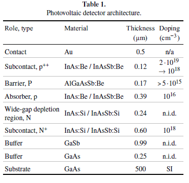
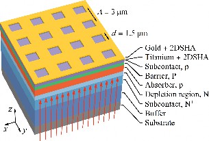
We propose to base the plasmon-enhanced infrared photodetector on a photodiode architecture with an InAs/InAsSb type-II superlattice (T2SL) absorber. The schematics of the device is shown in Fig. 1, and Table 1 includes a brief description of its component layers. The device is flicker-noise free and features high detectivity that may be further improved by utilizing plasmonic structure.
The InAs/InAsSb type-II superlattice (T2SL) was chosen as an active material because its band gap and corresponding cut-off wavelength may be easily tuned in a wide range between 4 μm and 16 μm by changing the superlattice period and the InAs/InAsSb layer thickness ratio while the InAsSb composition adjustment enables balancing strain in the structure [10–12]. Another advantage of this material compared to bulk InAsSb is lower Shockley–Read–Hall recombination due to reduced defect density. It is also easier to grow than InAs/GaSb superlattice [13].

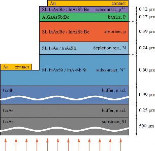
The heterostructure was deposited by molecular beam epitaxy (MBE) on the GaAs semi-insulating substrate. This semiconductor is transparent in the wide range between 1 μm and 18 μm which enables backside illumination for performance improvement. On the substrate, a GaSb buffer is grown to provide a proper lattice constant for InAs/InAsSb T2SL deposition. The heterostructure consists of a highly doped N+ layer for bottom contact formation, a p-type absorber, where the signal photocarriers are generated, AlGaAsSb unipolar barrier that suppresses electron injection to the absorber, and a heavily-doped p++ layer providing low top contact resistance. Additionally, a low-doped N-type layer with the same band gap as the N+ contact layer was introduced between the absorber and N+ layer to move the depletion region into the broader-gap semiconductor and by that to reduce Shockley–Read–Hall and Auger generation in the absorber. The gold contact metallisation on p++ and N+ layers enables efficient signal collection from the detector structure.
Based on the deposited heterostructure, a test device without 2DSHA (with continuous gold layer on top) was fabricated using photolithography, mesa wet etching and galvanic deposition of gold. The detection chip was assembled on a thermoelectrical cooler, electrically connected by wire bonding and characterized. The aim of this experiment was to evaluate the performance of the heterostructure without 2DSHA as a reference for a detector improved for instance via plasmon enhancement.
Fig. 2 includes the measured J-V curves which show the drift and diffusion current domination around 0V, tunneling current for reverse bias and series resistance influence for forward bias. The detector exhibits 0V dynamic resistance of 0.28, 0.98 and 2.2 Ω·mm2 at 297 K, 230K and 210K respectively, which allows for fabricating a device with an area large enough for 2DSHA integration (e.g. 200 × 200 μm2) and a sufficiently high resistance for noiseefficient coupling with preamplifier.
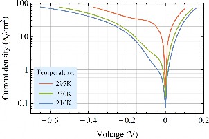
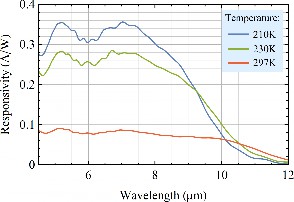
Fig. 3 shows the detector spectral characteristics measured using a FTIR spectrometer. The long-wavelength edge of the spectra (9-12 μm) corresponds to the absorption edge of the absorber material broadened by the Urbach tail. The cut-off wavelength decrease with cooling is caused by the negative temperature dependence of the InAs/InAsSb superlattice band gap [14]. The device exhibits 0.08, 0.25, 0.30 A/W responsivity and 3.2 · 107, 2.2 · 108, 4.2 · 108 cm · Hz1/2W-1 detectivity at wavelength of 8 μm and temperatures of 297 K, 230 K, 210 K, respectively.
The responsivity decrease with temperature is caused by the increase of parasitic series resistance contribution to total resistance. The detectivity drop is even stronger due to thermal noise increase with temperature. The lowresponsivity of the detector is caused byweak absorption of long-wavelength radiation in the absorber layer. Unfortunately, all materials optimized for the LWIR range, including the InAs/InAsSb T2SL, feature short diffusion lengths that constrain the transport of the photogenerated electrons and holes to contacts. To obtain efficient carrier collection, a very thin (390 nm in our case) absorber must be used. This results in weak absorption of infrared radiation which leads to the poor quantum efficiency of a conventional device. The solution may be to use plasmonic structures for absorption enhancement. To investigate such a possibility, we performed numerical simulations of the described semiconductor heterostructure integrated with a two-dimensional subwavelength hole array (2DSHA) in the top-contact metallisation.
Such a detector may be fabricated by a similar procedure as for the test device described before, based on photolithography, mesa etching, metallisation and assembly. However, the2DSHArequires a much higher resolution of lithography than a conventional detector structure. Therefore for fabrication of a detector with 2DSHA, electron-beam lithography or optimised UV lithography is necessary. Also, for series production ICP-RIE may be used instead of wet etching and sputtering rather than galvanic metallisation. Sputtering requires an additional titanium wetting layer, approx. 5 nm thick, between semiconductor and gold. The processed wafer shall be diced into chips by a saw with a diamond blade. To enable backside illumination flip-chip assembly on a sapphire or silicon carrier is performed prior to mounting on a thermoelectric cooler, wire bonding and packaging.
Ellipsometric measurement results
The analyzed architecture relies on the excitation of various electromagnetic modes, thus the knowledge of the complex refractive indexes of all the constituent layers is of high importance. This is especially true for the absorber which consists of a multilayer superlattice whose optoelectronic properties depend on its material and structural parameters. To extract the optical parameters of the fabricated samples we employed infrared spectroscopic ellipsometry with the use of IR-VASE Mark II Woollam ellipsometer. The measurement is based on acquiring the ellipsometric parameters 𝛹(𝜆) and 𝛥(𝜆), which correspond to the ratio of the reflection coefficients and the phase difference between the p- and s-polarization components of the incident beam. The ellipsometric curves were measured in a spectral range from 1.7 μm to 30 μm and incidence angles from 55 to 75 degrees with a 5-degree step. The optical parameters (complex refractive index) were extracted based on the isotropic model taking into account all the elements of the sample. The absorber layer was prepared for the measurements on the single-side polished GaAs wafer with an additional GaSb layer. The thickness of subsequent layers was measured by scanning electron microscopy. Optical parameters of the substrate were measured prior to the experiment and their perfect match to the Woollam database was confirmed.

The complex refractive index of the absorber is modelled with the use of the General Oscillator model where the real part of the refractive index is described by the 𝜖∞ that is permittivity at an infinite frequency and two poles that are equivalent to a Lorentz oscillator with zero broadening, that are placed outside of the measured spectral range. The imaginary part of the refractive index in the IR is described by two Tauc-Lorentz oscillators. The roughness is modeled as an effective layer assuming 50% content of voids and underlying material which optical constants are calculated with the use of Bruggeman effective medium approximation. Fig. 4 shows ellipsometric curves (solid lines) with the model (black dashed lines) fitted to the experimental data. Oscillations in both curves come from the interference effect occurring in the sample, which proves that the layer is semi-transparent, while the lower contrast of the fringes in the short wavelength range indicates an increase of the absorption in the material.

Fig. 5 presents a summary of the dispersion characteristics of the absorber, p++, N and N+ superlattices as well as of the AlGaAsSb barrier, GaSb buffer and GaAs substrate. The optical parameters of p++ material are considered to be the same as those of the absorber due to the identical design (InAs/InAsSb layers thickness and composition) of both superlattices. The dependencies of the refractive and extinction indices have been used in all further calculations included in this work. Since we are interested in obtaining the maximal absorptance within the absorber layer, it would be most desired to have an absorber with a high extinction index at the targeted wavelength range, whereas all other components of the detector should have the extinction index as low as possible. However, the absorptance within the absorber layer also depends on the actual light intensity within its volume. For instance, the Au mirror on top of the detector partly increases intensity within the absorber by adding the reflected wave contribution to intensity. Creating Fabry-Pérot modes may also increase absorptance at specific wavelengths. Adding a grating on top of the detector opens more possibilities, allowing for coupling reflected light into spatially localized modes within specific layers or at the layers boundaries
From a glimpse at the refractive index dispersion data, we see that GaSb has the largest refractive index among all materials compared. Therefore the GaSb buffer layer is a potential candidate for the core region of the lowest order waveguide modes that may be excited within the multilayer structure. A metal-dielectric boundary on the other hand may support SPP modes.
Dispersion of surface plasmon modes, Sommerfeld- Zenneck surface wave modes and planar waveguide modes coupled by the 2DSHA
In this section we estimate the resonant wavelengths of the detector integrated with the 2DSHA without performing a full 3D numerical modelling. In fact, the coupling conditions for the excitation of SPP modes and waveguide modes in specific layers of the detector may be found approximately by substituting the grating equation into the analytical dispersion formula of a SPP wave, or into the implicit characteristic equation of a waveguide, respectively. There is an obvious limitation to this approach. If a SPP mode or waveguide mode spreads over several layers of the detector, the analytical dispersion formulas are only approximate. Additionally, two or more modes with the same polarization may couple modifying the modal wavelengths. Despite the limitations, this approach is sufficient for predicting approximate resonant wavelengths and associating them with the excitation of SPP or waveguide modes.
\[ \begin{gathered} \beta_{2 D S H A}=\frac{2 \pi}{\Lambda} \sqrt{m_x^2+m_y^2} \text {, where } m_x, m_y \in \mathbb{Z} \text {. } \end{gathered} \] (1)
In a medium with a refractive index 𝑛, these modes are evanescent if 𝛽2𝐷𝑆𝐻𝐴/𝑘0 > 𝑛, where 𝑘0 = 2𝜋/𝜆. In our case, 𝛬 = 3 μmso the non-zero diffraction orders (𝑚2 𝑥+𝑚2 𝑦 > 0) become evanescent in air when 𝜆 > 3 μm. Orders that are evanescent also within the semiconductor structure may be potentially coupled to waveguide or SPP modes. If these modes are spatially located in the vicinity of the absorber they may contribute to enhanced absorption and increased detector quantum efficiency.
Let us consider an idealised infinite planar boundary between two half-spaces, one containing a metal and the other containing a dielectric or semiconductor. Assuming the p-polarisation, a SPP mode may be excited at the boundary and its dispersion relation is [2]
\[ \begin{gathered} \beta_{s p p}=k_0 \sqrt{\frac{\epsilon_m(\lambda) \epsilon_d(\lambda)}{\epsilon_m(\lambda)+\epsilon_d(\lambda)}} \end{gathered} \] (2)
where 𝜖𝑚 and 𝜖𝑑 are the complex permittivities of the two materials. The SPP modes may be excited using a grating at wavelengths for which the real parts of 𝛽 𝑠𝑝𝑝 and 𝛽2𝐷𝑆𝐻𝐴 match. Depending on the grating’s pitch, the coupling may occur at the surface plasmon (SP) resonance or other wavelengths, and the coupling condition may be satisfied at multiple wavelengths corresponding to different diffraction orders (𝑚𝑥, 𝑚𝑦). Equation (2) describes a surface wave only above the wavelength corresponding to the metal’s plasma frequency. The surface plasmon polariton is excited at a higherwavelength, when Re(𝜖𝑚(𝜆)+𝜖𝑑 (𝜆)) ≈ 0. At the SP resonance the surface wave becomes strongly localized in the transverse and horizontal directions, and exhibits decreased phase and group velocities. On the other hand, the long-wavelength asymptomate of the SPP dispersion equation (2) is simply the dispersion relation of the dielectric 𝛽 𝑠𝑝𝑝 (𝜆) ⪆ 𝑘0 √︁ 𝜖𝑑 (𝜆) (because at high wavelengths |𝜖𝑑 (𝜆)/𝜖𝑚(𝜆) | ≪ 1). In this regime, (when 𝛽 𝑠𝑝𝑝 (𝜆) ⪆ 𝑘0 √︁ 𝜖𝑑 (𝜆)) the corresponding surface wave is called a Sommerfeld-Zenneck wave [15, 16] . Sommerfeld- Zenneck waves do not exhibit decreased group and phase velocities, they are weakly localized at the metal-dielectric boundaries and resemble plane waves propagating within the dielectric, parallel to the interface, though they decay with distance from the interface. Despite the differences between Sommerfeld-Zenneck waves and the strongly localized surface plasmon polaritons, in a broader sense, all surface waves described by (2) are sometimes called SPP waves.
For the detector considered in this paper, the SPP may be exited at the gold surface. Additionally, a very thin, approx. 5 nm thick, titanium adhesive layer may also play some role in the surface wave excitation.Fig. 6(a) shows the SPP dispersion at the Au-p++ interface. For comparison, we also include the dispersion relation at a Ti-barrier boundary. Overprinted in Fig. 6(a) are the modes generated by the grating. Note that the 𝛽2𝐷𝑆𝐻𝐴/𝑘0 ranges where these modes are evanescent are above the dotted lines with the respective refractive index of the dielectric material. Crossings between the grating modes and SPP modes indicate the possible coupling conditions. The surface plasmon resonance wavelength is in the UV/VIS range for the gold surface and at 𝜆 ≈ 4.5 μmfor the Ti surface. Avoiding the SP resonance may be advantageous. In fact, the SP resonance would incur high light dissipation due to ohmic losses in the metal. Additionally, due to the strong SPP localization, the highest field enhancement may occur away from the absorber region. Finally, for a given metal, the possibility of modifying the resonant wave length is narrow. These limitations may be alleviated by the use of “designer” epitaxial plasmonic metals [5], which is not considered in the present work. In our case, at the LWIR/MWIR wavelengths the detector retains a resonant behaviour because the resonant conditions are set by the grating’s pitch rather than due to the SP resonance. The dispersion relation of the SPP at the Au-p++ boundary approximately matches the dispersion relation of the refractive index of p++ SL (See Fig. 6(a)). This indicates that the SPP wave in the LWIR/MWIR range reaches the long-wave asymptotic form, and is a Sommerfeld-Zenneck wave.
Further insight into the SPP modes may be obtained from the characteristic length scales associated with the SPP wave, which are plotted in Fig. 6(b). The three characteristic plasmon dimension measures are calculated as [2]
\[ \begin{gathered} l(k)=|\operatorname{Im}(k)|^{-1} \end{gathered} \] (3)
w√︃ith 𝑘 = 𝛽 𝑠𝑝𝑝 for the propagation range,
\[ \begin{gathered} k=\sqrt{k_0^2 \epsilon_m-\beta_{s p p}^2} \end{gathered}\]
for the penetration depth into the metal and\[ \begin{gathered} k=\sqrt{k_0^2 \epsilon_d-\beta_{s p p}^2} \end{gathered}\]
for the penetration depth into the semiconductor, respectively. The SPP propagation length exceeds 10 μmand approaches 100 μmfor higherwavelengths. SPP penetration into the metal is on the order of tens of nanometers, while the penetration depth into the semiconductor material is in the order of a few micrometers. The SPP propagation length exceeds 10 μmand approaches 100 μmfor higherwavelengths. SPP penetration into the metal is on the order of tens of nanometers, while the penetration depth into the semiconductor material is in the order of a few micrometers.Apart from exciting SPP modes, the 2DSHA may also couple light to guided modes. The GaSb buffer layer has the highest refractive index upon all layers of the detector and should support at least the fundamental TE0 and TM0 slab waveguide modes. The guided modes supported by an idealised asymmetric slab waveguide consisting of a GaSb core and GaAs and N+ claddings are plotted in Fig. 7(a). The wavelengths satisfying the coupling conditions are also indicated. Likewise the Sommerfeld-Zenneck wave, also the guided waves have the penetration depths on the order of the detector thickness (See Fig. 7(b)).
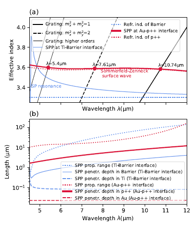
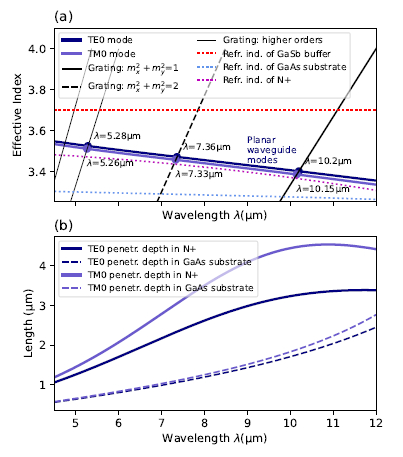
The coupling conditions marked in Fig. 6(a) and Fig. 7(a) indicate that the resonant wavelengths for specific grating modes appear in triplets, with the lowest wavelength mode originating from TM0 waveguide mode, the middle wavelength mode from the TE0 mode and the highest wavelength mode from the SPP (Sommerfeld-Zenneck) TM-polarized surface wave. The wavelengths of these triplets are (10.15 μm, 10.20 μm and 10.74 μm) for the lowest order grating order, and (7.33 μm, 7.36 μm and 7.61 μm), (5.26 μm, 5.28 μm and 5.4 μm) for subsequent two orders. Triplets from the two first grating modes are isolated while those from higher order grating modes may overlap. Within each triplet, the two TM-polarized modes may couple and their actual wavelengths may differ from the values predicted in this section. While the simply obtained results give some insight into the behaviour of light inside the detector, a refined analysis should be based on vectorial 3D modelling.
3D rigorous optical modelling of the detector
In this section, we focus on the detector with a 2DSHA and conduct its rigorous 3D optical modelling. Fig. 8 shows the detector schematics including the 55 nm thick Ti/Au layer with 2DSHA based on a square lattice with a pitch of 𝛬 = 3 μm put in place of a classical uniform top contact layer. We have performed FDTD and RCWA modelling of this structure. We begin by discussing the results and further in this section focus on the comparison between the two modelling approaches.
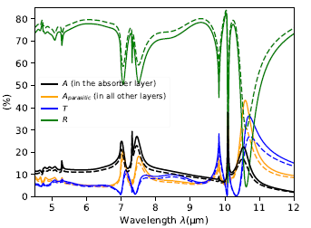
In Fig. 9 we show the transmittance and absorptance spectra of the detector obtained with RCWA and FDTD. The results are in good agreement. The first two mode triplets originating from the lowest order grating modes may be easily identified in the plot. For comparison, the reference results for a similar detector but with a uniform top contact layer are also shown. We observe a significant absorptance enhancement in the vicinity of these resonances (see the red and green curves in Fig. 9(a).)
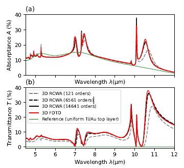
Table 2 includes a detailed comparison of the absorptance maxima locations, heights and widths (full width at half maximum - FWHM) obtained with RCWA and FDTD. Notably, the FWHMs range from 13 nm to several hundred nanometers. The main features of the resonances belonging to each triplet, including the spectral locations, polarizations and field profiles, allow to attribute the origins of corresponding modes predominantly to the TM0, TE0 and SPP (Sommerfeld-Zenneck) modes, respectively. More precisely, all modes are hybrid and each includes some contribution from the other polarization and some elements of the field profiles originating from the other two. In particular, coupling takes place between the two TM-polarized modes but the 2D grating is also capable of coupling different polarizations together.
Table 2.
Absorptance maxima calculated with RCWA and FDTD.
3D RCWA (𝑁 = 60, (2𝑁 + 1)^2 = 14641 orders).
𝜆 (nm) |
A (%) |
FWHM (nm) |
7010 |
24.9 |
135 |
7315 |
29.4 |
24 |
7453 |
27.1 |
145 |
9826 |
9.1 |
13 |
10086 |
38.0 |
30 |
10536 |
22.3 |
288 |
𝜆 (nm) |
A (%) |
FWHM (nm) |
6985 |
25.7 |
145 |
7309 |
28.1 |
27 |
7447 |
27.7 |
142 |
9804 |
9.4 |
25 |
10079 |
32.8 |
47 |
10529 |
23.9 |
273 |
The narrow central modes within each triplet come primarily from the TE0 guided mode and are located at wavelengths quite well predicted by the theoretical model from the previous section (RCWA predicts maxima at 10.086 μm and 7.315 μm, while the theoretical model at 10.20 μm and 7.36 μm). The long-wavelenth modes of the triplets primarily stem from the TM-polarised SPP modes. Their wavelengths are shifted downwards with respect to the theoretical model (RCWA gives maxima at 10.536 μm and 7.453 μm, while the theoretical model at 10.74 μm and 7.61 μm). Finally the modes originating from the TM0 waveguide mode have wavelengths shifted downwards significantly (RCWA gives maxima at 9.826 μm and 7.010 μm, while the theoretical model at 10.15 μm and 7.33 μm).
The most significant absorptance enhancement due to the 2DSHA takes place in the LWIR range and is related to the resonances at 10.086 μm and 10.536 μm. Fig. 10 shows selected field cross-sections obtained at these two wavelengths. The waveguide mode is mostly located in the GaSb buffer layer. Its exact effective index depends on the GaSb core thickness. On the other hand, the plasmonic mode is less dependent on the thicknesses of particular layers and its wavelength depends on the SPP dispersion (See Fig. 6).
Numerical simulations of the structure have been performed with FDTD [8] and RCWA [9]. The former was realized using commercial software [18], while the latter one with open-source PLaSK solver [19], developed partially by the authors of this paper. In particular, it implements the plane-wave reflection-transfer method [20, 21] which is equivalent to the RCWA, although it uses the reflection matrix transfer process [22] instead of scattering matrix to ensure numerical stability of the solution.
FDTD is a 3D vectorial time-domain finite-difference method that enables us to trace the time-evolution of a broadband pulse within an arbitrarily defined structure. Still, the structure has to be small due to the dependence of the computational requirements on the structure’s volume. As long as the simulated system is optically linear, a single FDTD simulation provides broadband information about the transmittance, reflectance or absorptance spectra. In practice, there is a trade-off between accuracy and the spectral width of the source, and in this work, a sequence of FDTD simulations is conducted in overlapping 8 or 16 THz ranges to determine the broadband spectra.
Conversely, RCWA is a 3D vectorial frequency-domain solver based on spatial 2D Fourier decompositions of the field and refractive index profiles. The simulated structure needs to be 2D-periodic and should have a layered composition in the third dimension but its volume may be arbitrarily large, as the numerical effort depends on the structure’s complexity rather than on its size. A single simulation provides information about a single frequency, thereby a sequence of simulations is required to find the entire transmission or reflection spectra. RCWA may be better suited for optimizing the structure at a particular wavelength [23, 24], as well as for analyzing spectrally narrow resonances. RCWA may be superior to FDTD in the modelling of tunnelling or mode coupling, as long as all relevant propagating and evanescent diffractive orders are included in the calculations.
The transmission values shown in Fig. 9(b) are computed directly by the RCWA. To determine the absorptance it is necessary to integrate the field in the absorber region. Parasitic absorptance in other components of the detector may have a significant contribution to the total absorptance, however without any effect on the overall quantum efficiency. Thanks to the orthogonality of the Fourier basis, the calculation of absorptance is straightforward. The absorbed energy flux is computed as
\[ P_A=\int_{\text {absorber }} \sigma \mathbf{E} \cdot \mathbf{E}^* d V \] (4)
where
\[ \sigma=\frac{2 \pi \operatorname{Im}(\epsilon) \epsilon_0}{\lambda} \] (5)
Neither FDTD nor RCWA performs well in the presence of metals. Modelling metals requires including a huge number of diffraction orders into RCWA calculations, and a deeply subwavelength sampling density as well as refined time-domain sampling in the case of FDTD.Yet, when properly set up, both FDTD and RCWA give consistent results.
As the RCWA method is directly based on the Fourier expansion of the electromagnetic field in horizontal directions, it is particularly well suited for the analysis of periodic structures, like the one presented in this paper. However, it also suffers from the undesired Gibbs phenomenon, which strongly deteriorates its convergence if the electric field vector is perpendicular to the grating grooves. For simple, one-dimensional gratings, this problem can be alleviated by using the inverse expansion [25]. In the case of a 2D array, the orientation of particular field components with respect to the grating edges is inconsistent along the computation domain, which makes direct application of the inverse rule impossible. One way to overcome this issue is the local separation of the electric field into perpendicular and parallel components [26-27]. However, they result in a non-uniform representation of the electric field as a sum of two representations, in which horizontal components 𝐸𝑥 and 𝐸𝑦 are both expanded using direct and inverse rules. While this approach improves the convergence for dielectric materials,we have noticed that it does not work well in the case of metallic grating. For this reason, we stick to the direct rule for both horizontal E-field components. This makes the convergence slower, which is illustrated inFig. 9 It can be seen that both the transmission and absorption of the incident wave stabilize above 40 𝑘-vector components in each direction, which gives the total number of (2 × 40 + 1)2 = 6561 considered diffraction orders (for practical implementation, this number is reduced by the factor of 4 due to the mirror symmetries along x and y axes.)

Absorbance maxima shown in Fig. 9(a) and listed in Table 2 correspond to the transmittance peaks (Fig. 9(b)). In particular, both peaks above 10 μm show characteristic Fano shape [28], however, they significantly differ in their Q-factors. This suggests that, whereas both resonances are Fano resonances, they show different natures. Indeed, the resonance around 10.536 μm corresponds to the excitation of an SPP (Sommerfeld-Zenneck) mode, while the resonance at 10.086 μm is due to the excitation of a waveguide mode, which can be seen in Fig. 10. The waveguide mode is laterally located under the air hole of the metallic grating and has a field distribution consisting of a single large blob. From the numerical point of view, its field expansion in the Fourier basis within the 𝑥𝑦-plane requires a smaller number of plane waves. This results in a fast convergence of RCWA. On the other hand, the SPP (Sommerfeld-Zenneck) mode – as the one resulting from strong interaction with metal – needs a good representation of high-order 𝑘-vector components and shows much slower convergence (See Fig. 9).
Approximate treatment of the substrate in simulations and adaptive selection of data points for RCWA calculations
Detector heterostructures are typically by several orders of magnitude thinner than the substrate. In our case, the thickness of the detector is on the order of 2 μm, while the thickness of the substrate counts in hundreds of micrometers. The easiest and most common approach to the modelling of a structure deposited on a substrate is to assume that the substrate is semi-infinite. If the substrate is included in a 3D FDTD simulation, such modelling would involve a macroscopic volume requiring immense computational resources. On the other hand, in the case of RCWA, the substrate only negligibly affects the computational cost. RCWA results for the substrate included in the model would exhibit strong and spectrally rapid Fabry-Pérot modulation. This modulation, also known as an optical fringing effect, is an important limitation in some applications, e.g. laser absorption spectrometry, but it is not the subject of this work. Nonetheless, the substrate strongly affects the performance of the detector due to the large value of the Fresnel intensity reflection coefficient for a normally incident wave at the boundary with air:
\[ R_0=\left|\frac{n_{\text {substr }}-1}{n_{\text {substr } r}+1}\right|^2 \] (6)
where 𝑛𝑠𝑢𝑏𝑠𝑡𝑟 is the complex refractive index of the substrate. For a GaAs substrate, 𝑅0 is approximately equal to as much as 30%.
Coverage of the substrate with an anti-reflective coating (ARC) is a simple remedy for the Fresnel reflections. In the absence of ARC we propose to apply a simple correction to the calculations involving a semi-infinite substrate, which accounts for multiple intensity reflections of the zeroth diffraction order from the substrate. The adjusted values of the reflection, transmission and absorption coefficients are given as
\[ \begin{aligned} & R^{\prime}=R_0+R\left(1-R_0\right)^2 /\left(1-R R_0\right) \\ & T^{\prime}=T\left(1-R_0\right) /\left(1-R R_0\right), \\ & A^{\prime}=A\left(1-R_0\right) /\left(1-R R_0\right), \end{aligned} \] (6)
where the primed symbols 𝑅′, 𝑇′, 𝐴′ include the correction, while 𝑅, 𝑇, 𝐴 come from the numerical calculations with a semi-infinite substrate. Equations (7) are based on the transmission and reflection coefficients of a non-coherent Fabry-Pérot etalon. Fig. 11 includes a plot showing how the transmittance, absorptance and reflectance spectra are affected by the presence of a finite substrate.
The computational costs of 3D FDTD and RCWA are at least on the order of 𝑂(𝑁4), where 𝑁 represents a quantity proportional to the sampling density for FDTD and the number of 𝑘-vector values in either of the two transverse directions forRCWA. While the implementation of the FDTD used in this work takes profit from a nonuniform mesh to speed up calculations, we also propose a method to reduce the computational time of RCWA. We have introduced a simple but highly efficient algorithm for the adaptive selection of wavelength data points for RCWA calculations. Adaptive point selection is illustrated in Fig. 12, which shows a part of the calculated absorptance spectrum.
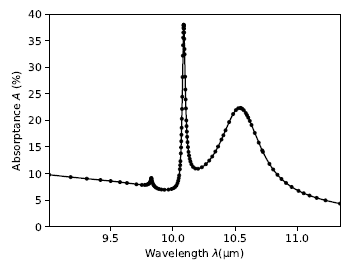
(Fig. 12 includes a magnified part of the absorptance spectrum calculated with 3D RCWA and shown in whole in Fig. 9(a). Fig. 12 additionally includes the calculation data points.) New wavelength values for RCWA calculations are selected by finding the wavelength at which the difference between linear and quadratic interpolation results is the largest. As a result, the actual sampling density varies depending on the local complexity of the calculated results, enabling us to describe the maxima having largely variant peak values and FWHMs with high fidelity, using only a moderate number of data points. In the case of the absorptance spectrum, the ratio of the average to minimal distance between the wavelength data points was on the order of 25–50 which is also an estimate of the speedup factor at which no significant decrease of accuracy is observed.
Conclusions
2D subwavelength hole array in a metallic film attached on top of a HOT LWIR photovoltaic detector heterostructure with an InAs/InAsSb T2SL absorber generates multiple evanescent diffraction orders in reflection. 3D RCWA and FDTD calculations enabled us to determine the resonant wavelengths at which the hybrid waveguide and SPP modes are excited contributing to enhancing absorptance in the absorber of the detector. The respective absorptance spectrum includes maxima differing significantly in magnitudes, FWHM, and internal field distributions posing a challenge for efficient numerical modelling. Modes with a predominantly TE0 waveguide nature are narrow banded exhibiting a typical Fano shape. On the other hand, the SPP modes with a Sommerfeld-Zenneck wave origin are spectrally broader and feature significant field enhancement in the vicinity of the metallic grating. The former may be accurately and efficiently modelled with RCWA, while for the latter modelling with FDTD is more efficient. Still, both FDTD and RCWA give consistent results. We have also proposed an adaptive way of data-point selection for reducing the RCWA calculation time as well as an approximate way of including the effect of the substrate on the reflectance and absorptance results applicable independently of the choice of the calculation method.
Hybridization of guided and SPP modes results in mode broadening offering the advantage of absorptance enhancement in broad wavelength ranges rather than at narrow spectral lines. Additionally, it gives a potential for tailoring the absorptance spectrum to a larger degree than only by exciting the SPP modes. According to our knowledge, infrared detectors with absorptance enhanced through joint excitation ofwaveguide modes and SPP-based Sommerfeld- Zenneck modes have not been studied before. We believe this work opens a path for exploring this mechanism that will lead to designing detectors with an increased quantum efficiency.
Acknowledgements
This study was conducted within the PEMIR project funded by The National Centre for Research and Development (Poland, grant no. POLTUR4/PEMIR/2/2021) and The Scientific and Technological Research Council of Turkey (grant no. 120N425) under the 4th call for bilateral projects in the frame of Poland-Turkey cooperation.
References
-
Piotrowski, J. & Rogalski, A. High-operating-temperature infrared photodetectors (SPIE, Bellingham, 2007). https://doi.org/10.1117/3.717228
-
Maier, S. A. Plasmonics: Fundamentals and Applications (Springer, 2007). https://doi.org/10.1007/0-387-37825-1
-
Tong, J., Tobing, L. Y., Qiu, S., Zhang, D. H. & Unil Perera, A. G. Room temperature plasmon-enhanced InAs0.91Sb0.09-based heterojunction n-i-p mid-wave in- frared photodetector. Appl. Phys. Lett. 113 2018https://doi.org/10.1063/1.5018012
-
Tong, J. C. et al. Surface plasmon enhanced infrared pho- todetection. Opto-Electron. Adv. 2 1–10 (2019). https://doi.org/10.29026/oea.2019.180026
-
Nordin, L., Petluru, P., Kamboj, A., Muhowski, A. J. & Wasserman, D. Ultra-thin plasmonic detectors. Op- tica 8 , 1545–1551 (2021).https://doi.org/10.1364/OPTICA.438039
-
Nordin, L., Muhowski, A. J. & Wasserman, D. High oper- ating temperature plasmonic infrared detectors. Appl. Phys. Lett. 120 (2022). https://doi.org/10.1063/5.0077456
-
Janaszek, A. et al. Plasmon-enhanced high operating tem- perature infrared photodetectors. In Staliu¯nas, K., Kuzmiak,
V. & Stefaniuk, T. (eds.) Metamaterials XIV , June, 27 (SPIE, 2023). https://doi.org/10.1117/12.2665259
-
Taflove, A. & Hagness, S. Computational Electrodynamics:
The Finite-Difference Time-Domain Method, Third Edition (Artec House Inc., Boston, 2005).
-
Moharam, M. G. & Gaylord, T. K. Rigorous coupled-wave analysis of planar-grating diffraction. J. Opt. Soc. Am. 71 , 811–818 (1981). https://doi.org/10.1364/JOSA.71.000811
-
Ting, D. Z. et al. InAs/InAsSb superlattice infrared detec- tors. Opto-Electron. Rev. 31, 1–7 (2023). https://doi.org/10.24425/opelre.2023.144565
-
Delmas, M. et al. High performance type-II InAs/GaSb superlattice infrared photodetectors with a short cut-off wavelength. Opto-Electron. Rev. 31, 4–9 (2023). https://doi.org/10.24425/opelre.2023.144555
-
Rafol, S. B. et al. Long wavelength type-II superlattice barrier infrared detector for CubeSat hyperspectral thermal imager. Opto-Electron. Rev. 31 (2023). https://doi.org/10.24425/opelre.2023.144569
-
Ting, D. Z. et al. InAs/InAsSb Type-II Strained-Layer Su- perlattice Infrared Photodetectors. Micromachines 11, 958 (2020) https://doi.org/10.3390/mi1111095
-
Manyk, T. et al. Electronic band structure of InAs/InAsSb type-II superlattice for HOT LWIR detectors. Results Phys. , 1119–1123 (2018).
11 https://doi.org/10.1016/j.rinp.2018.11.030 -
Polo Jr, J. A. & Lakhtakia, A. Surface electromagnetic waves: A review. Laser Photonics Rev. 5 , 234–246 (2011). https: doi.org/10.1002/lpor.200900050
-
Sarkar, T. K., Abdallah, M. N., Salazar-Palma, M. & Dyab,W. M. Surface plasmons-polaritons, surface waves, and Zenneck waves: Clarification of the terms and a descrip- tion of the concepts and their evolution.
IEEE Trans. An- tennas Propag. , 77–93 (2017). https://doi.org/10.1109/MAP.2017.2686079
-
Kumar, S., Selvaraja & Sethi, P. Review on optical waveg- uides. In Emerging Waveguide Technology (IntechOpen, Ri- jeka, 2018). https://doi.org/10.5772/intechopen.77150
-
Lumerical Inc., FDTD: 3D Electromagnetic Simulator.
-
https://plask.app.
-
Dems, M., Kotyński, R. & Panajotov, K. Plane Wave Admit- tance Method - a novel approach for determining the elec- tromagnetic modes in photonic structures. Opt. Express, 3196 (2005). 13 https://doi.org/10.1364/opex.13.003196
-
Dems, M. Modelling of high-contrast grating mirrors. The impact of imperfections on their performance in VCSELs. Opto-Electron. Rev. 19 , 340–345 (2011). https://doi.org/10.2478/s11772-011-0027-1
-
Helfert, S. F. Numerical stable determination of Floquet- modes and the application to the computation of band
structures. Opt. Quantum Electron. 36 , 87–107 (2004).https://doi.org/10.1023/B:OQEL.0000015632.23175.40
-
Schlipf, J. & Fischer, I. A. Rigorous coupled-wave analysis of a multi-layered plasmonic integrated refractive index sensor. Opt. Express 29, 36201 (2021). https://doi.org/10.1364/oe.438585
-
Moharam, M. G., Gaylord, T. K., Pommet, D. A. & Grann,E. B. Stable implementation of the rigorous coupled-wave analysis for surface-relief gratings: enhanced transmittance matrix approach.
J. Opt. Soc. Am. A 12 , 1077 (1995). https://doi.org/10.1364/josaa.12.001077
-
David, A., Benisty, H. & Weisbuch, C. Fast factorization rule and plane-wave expansion method for two-dimensional photonic crystals with arbitrary hole-shape. Phys. Rev. B 73https://doi.org/10.1103/PhysRevB.73.075107, 1–7 (2006).
-
Antos, R. Fourier factorization with complex polarization bases in modeling optics of discontinuous bi-periodic struc- tures. Opt. Express 17, 7269 (2009). https://doi.org/10.1364/oe.17.007269
-
Fano, U. Effects of configuration interaction on intensities and phase shifts. Phys. Rev. 124, 1866–1878 (1961). http://doi.org/10.1103/PhysRev.124.1866.