Development of the hybrid distributed Bragg reflectors for mid-infrared applications
- Laboratory for Optical Spectroscopy of Nanostructures, Department of Experimental Physics, Faculty of Fundamental Problems of Technology, Wrocław University of Science and Technology, ul. Wybrzeże Wyspiańskiego 27, 50-370 Wrocław, Poland
- Department of Microelectronics and Nanotechnology, Faculty of Electronics, Photonics and Microsystems, Wrocław University of Science and Technology, ul. Janiszewskiego 11/17, 50-372 Wrocław, Poland
Article Info
Received 23 Nov. 2023
Received in revised form 14 Dec. 2023
Accepted 22 Dec. 2023
Available on-line 17 Jan. 2024
Keywords: Distributed Bragg reflector; mid-infrared; meatal coating; InP; GaAs; FTIR.
Abstract
In this study, an analysis of the optical performance of two types of distributed Bragg reflector structures based on GaAs and InP material systems was carried out. The structures were designed for maximum performance at 4 μm with their reflectivity achieving between 80 and 90% with eight pairs of constituent layers. To further enhance the performance of these structures, additional Au layers were added at the bottom of the structure with Ti precoating applied to improve the adhesivity of the Au to the semiconductor substrate. The optimal range of Ti layer thickness resulting in the improvement of the maximum reflectivity was determined to be in between 5 and 15 nm.
Introduction
Mid-infrared (MIR) spectral range, extending from 3 to 8 μm, has numerous applications in open-air communication [1] and optical gas sensing [2]. The former uses the atmospheric window within the MIR range (between 3 and 5 μm) for data transmission, offering an alternative to conventional fibre optic networks, while the latter uses strong absorption lines of various atmospheric components in that spectral region for their efficient detection and quantitative evaluation.
Detection of volatile substances such as hydrocarbons or aldehydes holds significance in fields such as process control, petrol industry, and environmental protection systems [3, 4], while the analysis of the composition of exhaled air has been proven useful in medical applications [5, 6]. One of the key requirements of the optical detection system is a specialised single-mode, spectrally narrow light source emitting within MIR spectral region, corresponding precisely to the absorption lines of investigated substances while maintaining exceptional optical beam quality.
A promising candidate for a light source in this spectral range is a vertical cavity surface emitting laser (VCSEL) due to several advantages over a standard edge-emitting laser. The most significant is its ability to achieve singlemode operation characterised by extended coherence, thanks to its reduced cavity cross-section area [7]. In singlemode VCSELs, the emission occurs from only one optical mode, leading to a narrow and precisely defined spectral linewidth. Additionally, their low-threshold current results in reduced energy consumption in comparison to their edge-emitting counterparts [8]. Moreover, due to their high tunability, the emission wavelength can be easily customised, facilitating the detection of multiple absorption lines in multi-gas sensing [9] and creating a sweep lightsource suitable for 3D optical imaging [10]. A crucial component in the construction of a VCSEL is the resonance cavity with beam amplification occurring over a very short distance due to the compact size of the structure. There are several reports of enhancing the emission from the active region through the application of photonic crystals [11, 12] or, as the authors have shown in their previous works [13], with monolithic high contrast gratings. In the second approach, however, it is required to use high-reflectivity reflectors, with the bottom mirror reflectivity being as high as possible. Distributed Bragg reflectors (DBRs) are among the few types of structures capable of concurrently providing high-reflectivity and spectral selectivity, making them a valuable component for application in various other semiconductor devices. The theoretical basis behind the device using monolithic high-contrast gratings and DBRs as the top and bottom reflectors, respectively, was presented in Ref. 14.
Resonant-cavity light-emitting diodes, when equipped with high reflectance structures, exhibit enhanced extraction efficiency, greater brightness, improved directionality, and superior spectral purity compared to conventional light-emitting diodes [15–17]. In the case of photodetectors, incorporating an optical cavity leads to increased responsivity and wavelength selectivity [18, 19]. Additionally, high-resolution optical filters, such as Fabry–Perot filters, are typically crafted using DBRs or metal mirrors [20]. Despite their diverse applications, the fabrication of semiconductor DBRs for the MIR spectral region remains a challenge, mainly owing to the considerable thickness of the DBR layers as for maximum reflectivity and selectivity, it is essential to maintain the thickness of each layer as close as possible to a quarter of the wavelength at which they are intended to operate. Significant thickness needed for MIR applications increases the probability of structural defects due to strain-related issues and complicates the process control. Preferred material systems for growing III-V semiconductor nanostructures designed to operate within MIR spectral range are GaSb and InAs. There are numerous reports of interband cascade lasers (ICL) within these material systems covering a broad spectral range from 2–8 μm [21, 22], as well as VCSELs employing ICLs as active regions operating at 3.4 μm [23] and 4 μm [24].
This paper seeks to address the challenge of fabricating MIR VCSELs using an alternative InP platform. In previous works, MIR GaAs-based DBRs with impressive characteristics, such as reflectivity above 80% and transmittance close to 0, have been successfully demonstrated [25–27]. While GaAs technology is more advanced and widely used, the construction of InP-based DBRs offers the advantage in terms of compatibility with InP-based emitters, eliminating the need for a bonding process and simplifying the device production process significantly. However, it is worth noting that despite the existing technological development of the material system, growing InP-based DBRs remains challenging, primarily due to the limited availability of material pairs with a high contrast of refractive indices. In many cases, the fabrication of InP-based DBRs necessitates the use of ternary alloys, which further complicates the control of the growth process. Consequently, the designs for InP-based DBRs in the MIR region have been limited and are found in only a few publications. One approach, as described in Refs. 28–31, involves the use of an air gap within the DBR to attain a significant contrast in the refractive index of the DBR layers. Alternatively, another strategy to address this challenge is the exploration of more intricate compound materials [32, 33].
In this study, the authors conduct a comparison between InGaAs/InP DBR mirrors and more established AlAs/GaAs material system, both of which have previously been successfully designed for the MIR region. The growth of InP-based DBRs, as presented in this work, has historically posed challenges due to the need for precise control over single percent composition variations within selected materials and the demand for significant layer thickness with a high number of layers. Previously, InP-based DBRs were only applied for wavelengths of 1.5 μm [34, 35], 1.9 μm [36], and up to 2.5 μm [32]. Ultimately, the authors explored the approach that has enabled the attainment of a high level of reflectivity with the growth of only a few layers of InP-based DBRs by applying a thin Au film on the back of the sample. This solution allows to shift the stop band to longer wavelengths (4 μm) while retaining the simplicity of the few-layer deposition process. Up to now, such an approach has been used for a 1.5 μm VCSEL design using GaAs-Al(Ga)As DBR [37] and in a near-infrared (NIR) InGaAs/InP single-photon avalanche diode [38]. To further enhance the quality of the DBR-metal interface, additional Ti pre-coating was applied, as it has been shown that it may promote the adhesion of the Au layer to the semiconductor substrate [39].
Materials and methods
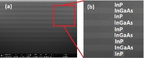
The samples were grown using a metalorganic vapour phase epitaxy (MOVPE) within a 3 × 2” CCS Aixtron system. In the process, TMIn, TMGa, and TMAl were used as the group III precursors for indium, gallium, and aluminium, respectively. For group V elements, phosphorus, and arsenic, 100% PH3 and 100% AsH3 were used as sources. The carrier gas flow, which is pure hydrogen, through the TMIn source was kept at a constant level during growth of the InP and InGaAs layers, resulting in growth rates of 0.6 nm/s and 1.05 nm/s, respectively. The growth temperature was maintained at 645 °C under a pressure of 100 mbar. To ensure lattice matching to the InP substrate, InGaAs layers were tailored with a 53% indium content. Precise layer thicknesses were confirmed through the SEM microscopy, with an example provided for InP shown in Fig. 1.

Following the MOVPE growth of the AlAs/GaAs and InGaAs/InP DBR structures, the samples were promptly transferred into a vacuum chamber of the evaporation system. Before metal deposition, the samples were subjected to a 24-hour vacuum treatment within the chamber. The metallisation process was executed using a physical vapour deposition (PVD 225 by Kurt J. Lesker Company) system, which was equipped with a cryogenic pump and a scroll-type vacuum pump. The gold and titanium metal layers were deposited onto the DBR, as illustfrated in Fig. 2, under high-vacuum conditions with a base pressure maintained below 10-6 mbar. While the Aumetal layer was deposited (100 nm for all samples) using aresistive thermal evaporator, the Ti layer was appliedthrough an electron beam evaporator. The thickness (5–20 nm) of the metal layers was quantified using a quartzcrystal microbalance monitoring system.
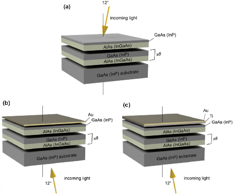
Reflectance measurements were conducted using avacuum Fourier transform infrared spectrometer (FTIR),specifically Bruker Vertex 80v [40–42]. Over the years,FTIR spectroscopy has been widely acknowledged for itsadvantages compared to dispersive setups [43, 44]. Toenable rapid and extensive data acquisition, a rapid scanmode was used in conjunction with a polychromatic lightsource (a glow bar) for these measurements. Parabolicgolden mirrors were used to direct the light to theMichelson interferometer, which then focused the lightonto the sample at an angle of approximately 12° to normalincidence, creating a spot with a diameter of roughly 0.25 mm, as depicted in Fig. 2 in Ref. 45. After interactingwith the sample, the reflected light was directed towards anInSb detector cooled with liquid nitrogen, where it wasconverted into an electrical response and then intoa spectrum using fast Fourier transform (FFT). Thisresulted in spectra with a resolution of 1 cm-1 spanning thespectral range from 1.3 to 5.5 μm. As a referencereflectance, the silver mirror was used.
Results
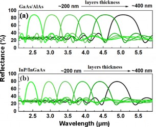
Fig. 3 illustrates the calculated reflectance spectra fortwo different DBR systems: eight pairs of GaAs/AlAs DBRin panel (a) and eight pairs of InP/InGaAs DBR in panel (b).These spectra depict how the stop band of the DBR can be tuned by varying the layer thickness, spanning the spectral range from 2.5 to 5.0 μm. It is noteworthy that both systems maintain a consistent reflectivity maximum, with the GaAs/AlAs DBR achieving around 90% and the InP/InGaAs DBR achieving approximately 80%. In the authors’ calculations, the thickness of the layers was adjusted to meet the criteria that each repeated pair has a quarter-wave thickness, as defined by the equation nd = λ/4, where n represents the refractive index of the layer, d stands for the thickness of the layer, and λ denotes the wavelength of light (at the stop band).
The enhancement of the stop band reflection is mainly achieved by increasing the number of layer pairs within the DBR. Fig. 4 shows the calculated reflectance spectra for two types of DBR: GaAs/AlAs DBR in panel (a) and InP/InGaAs DBR in panel (b), specifically designed for a 4 μm wavelength. These graphs demonstrate how the shape and peak intensity of the reflectivity spectra evolve with the incremental addition of DBR pairs. The characteristic spectral shape of the DBR can be observed consistently starting from eight pairs, and the maximum reflectivity reaches approximately 97% at around 4 μm, which is achieved with 12 pairs of combined layers. The results presented in Fig. 3 and Fig. 4 introduce two distinct DBR types based on GaAs and InP. These findings hold promise for potential applications in MIR optoelectronics. It is important to note that while using AlAs/GaAs requires advanced bonding procedures to integrate them with devices grown on currently popular MIR semiconductor substrates, InGaAs/InP DBRs are inherently compatible with the commonly used InP substrate in the MIR domain. Two commercially available software were used in our calculations, namely Filmetrics Reflectance Calculator and Lumerical. The calculations were based on materials parameters available at https://refractiveindex.info/ and https://www.filmetrics.com and were performed at room temperature. The nominal thickness was modified by around 2% to achieve the best agreement between the experiment and calculations.
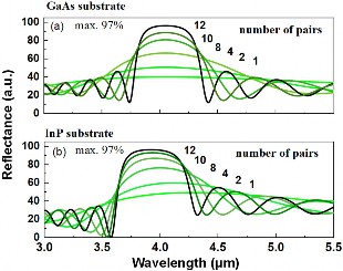
In the authors’ fabrication procedure, a DBR designed for a 4 μm wavelength was selected, which consists of eight pairs of AlAs/GaAs and eight pairs of InGaAs/InP based on the calculations presented in Fig. 3. The nominal values of thicknesses were presented in Table 1.
Table 1.
The nominal thicknesses of investigated DBRs layers.
Material |
GaAs |
AlAs |
InP |
InGaAs |
Thickness of layers [nm] |
303 |
351 |
324 |
274 |
An 8-pair design of the DBR was chosen intentionally to be cost-efficient and clearly assess the expected improvement of the reflectivity coefficient by application of metallic layers with no need for growing 20 or more pairs. In Fig. 5, panel (a), the authors present both calculated (green curve) and measured (black curve) reflectance spectra for the AlAs/GaAs DBR. In panel (b), the authors display the measured reflectance spectra (from the substrate side) for the same DBR, shown as the lower black curve. Additionally, the authors show the reflectance spectra for the DBR coated with an Au layer (lower green curve), a modified DBR structure with thickness of the last layer doubled (higher black curve), and Au-coated modified DBR (higher green curve). Upon analysis of the two lower curves in panel (b), it is evident that the reflectivity coefficient falls significantly below the projected value.

This discrepancy is primarily attributed to free-carrier absorption, a consequence of growing the structure on a doped GaAs substrate. Furthermore, it is evident that the application of thin layers of gold enhances the overall reflectivity. However, this enhancement comes at the cost of losing the characteristic shape of the DBR. This effect is a consequence of unintended light confinement between the Au layer and the DBR, leading to the opposing behaviour of the structure. Between the metal layer (below the plasma frequency) and the DBR, there is a possibility of electromagnetic mode confinement arising from the photonic stop band of the mirror, not the negative dielectric constant, as typically observed in regular plasmon-polariton phenomena. This phenomenon was initially described as a Tamm plasmon and observed in DBRs designed for NIR applications [46]. To address this challenge, the authors recalibrated the DBR design and doubled the thickness of the last layer in the DBR to eliminate the confinement. Additionally, the authors grew the structures on undoped GaAs substrates to reduce the number of free carriers and enhance transmittivity through the substrate. Although the reflectance spectrum is not yet optimized (black upper curve), the correct shape and high reflectivity of approximately 92% are achieved after applying the Au layer (top green curve).
DBRs with a different material combination were also fabricated, consisting of eight pairs of InGaAs/InP. In Fig. 6, panel (a), both calculated (green curve) and measured (black curve) reflectance spectra for the InGaAs/InP DBR are presented. Like the AlAs/GaAs DBR discussed earlier, the application of a gold layer on top of the DBR without any modification did not yield the desired results. Thus, the authors started with an already modified DBR design, following a similar approach as with the previous GaAs-based DBRs.
In Fig. 7, panel (b), the measured reflectance spectra (from the substrate side) for the modified DBR were displayed, depicted as a lower black curve, and the modified DBR additionally coated with an Au layer, presented as the top green curve.

As observed, following the same procedure as with the GaAs/AlAs DBR, the characteristic shape of the DBR in the spectra (black curve), which was subsequently restored upon applying the Au layer, was initially lost. Additionally, there is a notable increase in reflectance, with a reflectivity reaching up to 75%. These samples were also grown on undoped substrates, although some level of free-carrier absorption may be still occurring, potentially accounting for the decrease in reflectance.
Further enhancements in reflectivity were achieved by growing the modified InGaAs/InP DBR with a Ti pre-coating before the deposition of the Au layer [as shown in Fig. 2(c)]. In Fig. 7, measured reflectance spectra for the sample with only the Au layer (solid black curve) and with varying thicknesses of Ti pre-coating, ranging from 5 to 20 nm were presented. In comparison to the sample without the pre-coating, the 5 to 15 nm thickness range leads to a substantial improvement in reflectivity. Moreover, the effect appears to maximize for 10 nm of Ti, as increasing the thickness beyond this value actually reduces the reflectivity. The maximum reflectivity values as a function of Ti layer thickness are presented in the inset of the graph.

The observed improvement of over 10% in reflectivity with an additional application of thin Ti layers is unexpected, considering that gold has a higher-reflectivity coefficient. The deposition of metallic layers on semiconductors can be imperfect, especially when considering the atomic scale. Several factors may explain these unconventional experimental results. Most prior research has primarily focused on the influence of adhesion layers on gold deposition from an electrical perspective. The authors, in their work, considered the optical properties associated with the application of such layers to enhance the reflectivity.
Several noteworthy topics deserve mentioning in this context:
-
A thin, continuous layer of titanium plays a crucial role in promoting the adhesion of gold to the semiconductor surface. It also impacts the texture of the gold layer, resulting in smaller grain sizes compared to bulk gold material [39].
-
The reflectance at the interfaces, particularly the Ti/InP and Ti/Au interfaces, differs from that at the Au/InP interface due to variations in the chemical bonds. Titanium is known for its high reactivity, contrasting with gold, which has a more inert nature. These distinct chemical properties can lead to differences in reflectance properties at these interfaces [47].
-
The titanium layer can act as a barrier, preventing or limiting the diffusion of gold atoms into the epitaxial semiconductor structure. This is an important consideration for maintaining the integrity of the semiconductor materials and their performance [48, 49].
The observed experimental phenomenon represents a compelling area for further investigation, motivating extended studies involving new samples and the application of other metals. Such studies have the potential to provide a deeper understanding of this effect and its underlying mechanisms. Significant implications for the design of highly reflective mirrors, particularly within the context of structures featuring devices with resonant cavities, are underscored by the notable improvement in reflectivity, even at the modest level of 10%. The ability to reach high-reflectivity levels while simultaneously reducing the thickness of the entire device can have substantial benefits for the performance of optoelectronic devices.
Conclusions
In this study, AlAs/GaAs and InGaAs/InP DBRs designed for a 4 μm wavelength were successfully fabrica-ted. InP-based DBR has the potential to serve as a bottom reflector in a hypothetical VCSEL device comprising hybrid-DBR, quantum cascade laser core, and monolithic high-contrast grating designed for MIR emission. These DBRs, comprising only eight pairs, achieved around 90% and 80% reflectivity, respectively. The authors have also demonstrated that the number of layer pairs in the DBR can be effectively reduced by the application of metallisation layers. This reduction is particularly significant in the MIR spectral range, where the use of thick layers near the total thickness limits is often necessary.
Authors’ statement
Research concept and design, M.Mo. and M.B.; collection and/or assembly of data, M.Mi., M.R., T.S., A.Ł.; data analysis and interpretation, M.Mi., W.M.; writing the article, M.Mi. and M.Mo.; critical revision of the article, M.R. and T.S.; final approval of the article, M.Mo.
Acknowledgements
This work was supported by the Polish National Science Centre grant No. 2019/33/B/ST7/02591
References
-
Mikołajczyk, J., Weih, R. & Motyka, M. Optical wireless link operated at the wavelength of 4.0 µm with commercially available interband cascade laser. Sensors 21, 4102 (2021).https://doi.org/10.3390/s21124102
-
Sigrist, M. W. Air monitoring by spectroscopic techniques. Chemical analysis. (Wiley: New York, 1993).
-
Kluczynski, P. et al. Detection of acetylene impurities in ethylene and polyethylene manufacturing processes using tunable diode laser spectroscopy in the 3-μm range. Appl. Phys. B 105, 427–434 (2011).https://doi.org/10.1007/s00340-011-4645-6
-
Tittel, F. K., Richter, D. & Fried, A. A. Mid-Infrared Laser Applications in Spectroscopy. in Solid-state mid-infrared laser sources. Top. Appl. Phys. (eds. Sorokina, I. T. & Vodopyanov, K. L.) 89, 458–529 (Springer, 2003). https://doi.org/10.1007/3-540-36491-9_11
-
Risby, T. H. & Tittel, F. K. Current status of midinfrared quantum and interband cascade lasers for clinical breath analysis. Proc. SPIE. 49, 111123 (2010). https://doi.org/10.1117/1.3498768
-
Wang, C. & Sahay, P. Breath analysis using laser spectroscopic techniques: breath biomarkers, spectral fingerprints, and detection limits. Sensors 9, 8230–8262 (2009). https://doi.org/10.3390/s91008230
-
Guan, B., Li, P., Arafin, S., Alaskar, Y. & Wang, K. L. Investigation of single-mode vertical-cavity surface-emitting lasers with graphene- bubble dielectric DBR. Photonics Nanostruct. 28, 56–60 (2018).https://doi.org/https://doi.org/10.1016/j.photonics.2017.07.005
-
Koyama, F. Recent advances of VCSEL photonics. J. Light. Technol.24, 4502–4513 (2006).https://doi.org/10.1109/JLT.2006.886064
-
Wang, J., Sanders, S. T., Jeffries, J. B. & Hanson, R. K. Oxygen measurements at high pressures with vertical cavity surface-emitting lasers. Appl. Phys. B 72, 865–872 (2001).https://doi.org/10.1007/s003400100539
-
Ansbæk, T., Chung, I.-S., Semenova, E. S., Hansen, O. & Yvind, K. Resonant MEMS tunable VCSEL. IEEE J. Sel. Top. Quantum Electron. 19, 1702306 (2013).https://doi.org/10.1109/JSTQE.2013.2257164
-
Liang, Y. et al. Room temperature surface emission on large-area photonic crystal quantum cascade lasers. Appl. Phys. Lett. 114, 31102 (2019).https://doi.org/10.1063/1.5082279
-
Yao, Y. et al. Improved power and far-field pattern of surface- emitting quantum cascade lasers with strain compensation to operate at 4.3 μm. Jap. J. Appl. Phys. 61, 052001 (2022).https://doi.org/10.35848/1347-4065/ac5dbb
-
Mikulicz, M. et al. Enhancement of quantum cascade laser intersubband transitions via coupling to resonant discrete photonic modes of subwavelength gratings. Opt. Express 31, 26898–26909 (2023). https://doi.org/10.1364/OE.496261
-
Janczak, M. et al. Threshold performance of pulse-operating quantum-cascade vertical-cavity surface-emitting lasers. Opt. Express 30, 45054–45069 (2022). https://doi.org/10.1364/OE.474086
-
Al-Saymari, F. A. et al. Electroluminescence enhancement in mid- infrared InAsSb resonant cavity light emitting diodes for CO2 detection. Appl. Phys. Lett. 114, 171103 (2019). https://doi.org/10.1063/1.5090840
-
Al-Saymari, F. A. et al. Mid-infrared resonant cavity light emitting diodes operating at 4.5 µm. Opt. Express 28, 23338–23353 (2020).https://doi.org/10.1364/OE.396928
-
Green, A. M., Gevaux, D. G., Roberts, C. & Phillips, C. C. Resonant-cavity-enhanced photodetectors and LEDs in the mid- infrared. Physica E Low Dimens. Syst. Nanostruct. 20, 531–535 (2004). https://doi.org/https://doi.org/10.1016/j.physe.2003.09.004
-
Ghosh, S., Kumar, H., Mukhopadhyay, B. & Chang, G.-E. Design and modeling of high-performance DBR-based resonant-cavity- enhanced GeSn photodetector for fiber-optic telecommunication networks. IEEE Sens. J. 21, 9900–9908 (2021).https://doi.org/10.1109/JSEN.2021.3054475
-
Kumar, H., Pandey, A. K. & Lin, C.-H. Optimal design and noise analysis of high-performance DBR-integrated lateral germanium (Ge) photodetectors for SWIR applications. IEEE J. Electron Devices Soc. 10, 649–659 (2022). https://doi.org/10.1109/JEDS.2022.3195210
-
Al Sayem, A. & Rahman, M. S. Tunable Fabry Perot Filter Using All-Dielectric Multilayer Anisotropic Metamaterial in The Mid- Infrared Frequency Range. in 9th International Conference on Electrical and Computer Engineering (ICECE) 361–364 (IEEE, 2016). https://doi.org/10.1109/ICECE.2016.7853931
-
Bauer, A. et al. Emission wavelength tuning of interband cascade lasers in the 3–4 µm spectral range. Appl. Phys. Lett. 95, 251103 (2009). https://doi.org/10.1063/1.3270002
-
Dallner, M., Hau, F., Höfling, S. & Kamp, M. InAs-Based Interband-Cascade-Lasers in the 6-7 µm Wavelength Range. in International Semiconductor Laser Conference 42–43 (IEEE, 2014).https://doi.org/10.1109/ISLC.2014.154
-
Bewley, W. W. et al. Room-temperature mid-infrared interband cascade vertical-cavity surface-emitting lasers. Appl. Phys. Lett. 109, 151108 (2016). https://doi.org/10.1063/1.4964840
-
Veerabathran, G. K., Sprengel, S., Andrejew, A. & Amann, M.-C. Room-temperature vertical-cavity surface-emitting lasers at 4 μm with GaSb-based type-II quantum wells. Appl. Phys. Lett. 110, 71104 (2017). https://doi.org/10.1063/1.4975813
-
Palmer, C., Stavrinou, P. & Whitehead, M. Mid-infrared (λ∼2–6 µm) measurements of the refractive indices of GaAs and AlAs. Semicond. Sci. Technol. 17, 1189 (2002).https://doi.org/10.1088/0268-1242/17/11/310
-
Asano, T., Hu, C., Zhang, Y., Liu, M., Campbell, J. C. & Madhukar, A. Design consideration and demonstration of resonant-cavity- enhanced quantum dot infrared photodetectors in mid-infrared wavelength regime (3–5 µm). IEEE J. Quantum Electron. 46, 1484– 1491 (2010). https://doi.org/10.1109/JQE.2010.2052351
-
Perner, L. W. et al. Simultaneous measurement of mid-infrared refractive indices in thin-film heterostructures: Methodology and results for GaAs/AlGaAs. Phys. Rev. Res. 5, 33048 (2023). https://doi.org/10.1103/PhysRevResearch.5.033048
-
Suwito, G. R., Mojaver, H. R. & Quitoriano, N. J. Air Gap/InP Distributed Bragg Reflectors for Mid-Infrared Applications. in OSA Advanced Photonics Congress (AP) 2020 (IPR, NP, NOMA, Networks, PVLED, PSC, SPPCom, SOF) (eds. Caspani Tauke- Pedretti, A., Leo, F. & Yang, B. L.) M4G.4 (Optica Publishing Group, 2020). https://doi.org/10.1364/NOMA.2020.NoM4G.4
-
Yoshinaga, H. et al. Mid-Infrared quantum cascade laser integrated with distributed bragg reflector. Proc. SPIE 9755, 97552V (2016). https://doi.org/10.1117/12.2212332
-
Hashimoto, J. I. et al. Mid-infrared quantum cascade laser integrated with distributed bragg reflector. SEI Tech. Rev. 85, 59–64 (2017). https://sumitomoelectric.com/sites/default/files/2020-12/download_documents/85-12.pdf
-
Cheng, L. & Choa, F.-S. Design and operation of mid-IR integrated DBR tunable lasers. in Proc. SPIE 7953, 79531P (2011). https://doi.org/10.1117/12.875680
-
Sprengel, S. et al. Continuous wave vertical cavity surface emitting lasers at 2.5 μm with InP-based type-II quantum wells. Appl. Phys.Lett. 106, 151102 (2015). https://doi.org/10.1063/1.4917282
-
Boehm, G. et al. Growth of InAs-containing quantum wells for InP- based VCSELs emitting at 2.3μm. J. Cryst. Growth 301–302, 941–944 (2007). https://doi.org/https://doi.org/10.1016/j.jcrysgro.2006.11.098
-
Yue, A.-W., Wang, R.-F., Xiong, B. & Shi, J. Fabrication of a 10 Gb/s InGaAs/inp avalanche photodiode with an AlGaInAs/InP distributed Bragg reflector. Chinese Phys. Lett. 30, 38501 (2013).https://doi.org/10.1088/0256-307X/30/3/038501
-
Duan, X., Huang, Y., Shang, Y., Wang, J. & Ren, X. High-efficiency dual-absorption InGaAs/InP photodetector incorporating GaAs/ AlGaAs Bragg reflectors. Opt. Lett. 39, 2447–2450 (2014).https://doi.org/10.1364/OL.39.002447
-
Mi, J. et al. Fabrication of InGaAs/InP DBR laser with butt-coupled passive waveguide utilizing selective wet etching. Proc. SPIE 9267, 92670Z (2014). https://doi.org/10.1117/12.2071526
-
Hofmann, W. High-speed buried tunnel junction vertical-cavity surface-emitting lasers. IEEE Photon. J. 2, 802–815 (2010). https://doi.org/10.1109/JPHOT.2010.2055554
-
Zhang, B. et al. High performance InGaAs/InP single-photon avalanche diode using DBR-metal reflector and backside micro- lens. J. Light. Technol. 40, 3832–3838 (2022). https://doi.org/10.1109/JLT.2022.3153455
-
Todeschini, M., Bastos da Silva Fanta, A., Jensen, F., Wagner, J. B. & Han, A. Influence of Ti and CR adhesion layers on ultrathin Au films. ACS Appl. Mater. Interfaces 9, 37374–37385 (2017). https://doi.org/10.1021/acsami.7b10136
-
Motyka, M. et al. Fourier transformed photoreflectance and photoluminescence of mid infrared GaSb-based type II quantum wells. Appl. Phys. Express 2, 126505 (2009). https://doi.org/10.1143/APEX.2.126505
-
Motyka, M. & Misiewicz, J. Fast differential reflectance spectroscopy of semiconductor structures for infrared applications by using Fourier transform spectrometer. Appl. Phys. Express 3, 112401 (2010). https://doi.org/10.1088/0957-0233/22/12/125601
-
Motyka, M. et al. Fourier-transformed photoreflectance and fast differential reflectance of HgCdTe layers. The issues of spectral resolution and Fabry–Perot oscillations. Meas. Sci. Technol. 22, 125601 (2011). https://doi.org/10.1088/0957-0233/22/12/125601
-
Hosea, T. J. C., Merrick, M. & Murdin, B. N. A new Fourier transform photo-modulation spectroscopic technique for narrow band-gap materials in the mid- to far-infra-red. Phys. Status Solidi 202, 1233–1243 (2005). https://doi.org/10.1002/pssa.200460908
-
Griffiths, P. & Haseth, J. Fourier Transform Infrared Spectrometry, Second Edition. (Wiley, 2007).
-
Gębski, M. et al. Monolithic high-index contrast grating: a material independent high-reflectance VCSEL mirror. Opt. Express 23, 11674–11686 (2015). https://doi.org/10.1364/OE.23.011674
-
Kaliteevski, M. et al. Tamm plasmon-polaritons: Possible electromagnetic states at the interface of a metal and a dielectric Bragg mirror. Phys. Rev. B 76, 165415 (2007). https://doi.org/10.1103/PhysRevB.76.165415
-
Ivey, D. G. & Jian, P. Metallurgy of ohmic contacts to InP. Can. Metall. Q. 34, 85–113 (1995).https://doi.org/10.1179/cmq.1995.34.2.85
-
Stareev, G., Künzel, H. & Dortmann, G. A controllable mechanism of forming extremely low‐resistance nonalloyed ohmic contacts to group III‐V compound semiconductors. J. Appl. Phys. 74, 7344– 7356 (1993).https://doi.org/10.1063/1.355002
-
Katz, A. et al. Pt/Ti/p‐In0.53Ga0.47As low‐resistance nonalloyed ohmic contact formed by rapid thermal processing. Appl. Phys. Lett. 54, 2306–2308 (1989).https://doi.org/10.1063/1.101110