The method for extracting defect levels in the MCT multilayer low-bandgap heterostructures
- Institute of Applied Physics, Military University of Technology, ul. gen. Sylwestra Kaliskiego 2, 00-908 Warsaw, Poland
Article Info
Received 18 Dec. 2023
Received in revised form 12 Jan. 2024
Accepted 16 Jan. 2024
Available on-line 18 Feb. 2024
Keywords: Deep-level transient spectroscopy (DLTS); traps; MOCVD; MCT
Abstract
A method for defects extraction for a mercury cadmium telluride (MCT) multilayer low-bandgap heterostructure is presented. The N+/T/p/T/P+/n+ epitaxial layer was deposited on a GaAs substrate by a metal-organic chemical vapour deposition (MOCVD). The absorber was optimized for a cut-off wavelength of 𝜆𝑐=6 μm at 230 K. Deep-level transient spectroscopy (DLTS) measurements were conducted for the isolated junctions of the N+/T/p/T/P+/n+ heterostructure. Three localised point defects were extracted within the p-type active layer. Two of them were identified as electron traps and one as a hole trap, respectively.
Introduction
Defects in semiconductors deform their band structure leading to the formation of extra energy levels within the bandgap. Those states capture carriers, shortening their lifetime. Many experimental factors must be known and controlled to grow high-quality mercury cadmium telluride (MCT) epitaxial layers meeting the infrared (IR) detectors requirements. For example, the substrate type/orientation and temperature during deposition process largely contrib-ute to the defects formation. Even though MCT is well known for its excellent IR sensitivity and performance, it still exhibits various types of defects that may have a negative impact on performance.
Hg vacancies have been listed as the major native point defects in MCT. Additionally, threaded and misfit dislocations [1–4], surface crater defects [5–7], stacking faults and twins [4, 6, 8], and pyramidal hillocks [2, 9] may be formed in the MCT structures.
Large-format and multi-colour IR focal plane arrays (FPAs) fabrication requires semiconductor materials exhibiting a low concentration of internal defects in epitaxial layers [2, 3]. Therefore, it is extremely significant to study the nature of defects and determine their parameters. The most commonly used method to investigate electrically active defects creating trap states within the semiconductor bandgap is a deep-level transient spectroscopy (DLTS) [10].
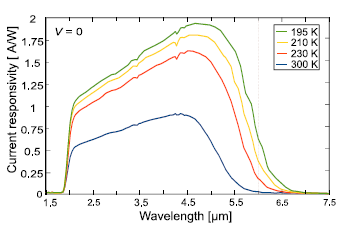
This work presents DLTS results and analysis of defects for a medium-wave infrared (MWIR) mesa geometry (400 μm × 400 μm) MCT multilayer heterostructure. The photodiode has been optimized to operate at a temperature of 230 K, and its architecture allows illumination from below through the N+ layer. The cut-off wavelength 𝜆𝑐 determined at 50% of the maximum signal value is approximately 𝜆𝑐=6 μm at 230 K. An increase in the bandgap with increasing temperature for the HgCdTe material shifts the cut-off limit towards shorter wavelengths (see Fig. 1)
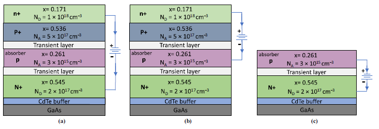
The N+/T/p/T/P+/n+ MCT epitaxial layer was grown on a CdTe buffer and a GaAs substrate by metal-organic chemical vapour deposition (MOCVD) [11, 12]. Three selected processing steps were performed to extract defects in the constituent layers. The procedure details will be described below.
Measurement technique
DLTS is the most powerful technique for studying electrically active defects in semiconductors, allowing to detect deep-energy levels by changing the space charge region capacitance under voltage being applied to the p-n junction. The voltage causes a corresponding variation in the depletion region width, which also causes a change in the junction capacitance. Additionally, the capacitance changes by capturing and emitting carriers from trap levels. Capacitance vs. time 𝑡 variation is given by [13]
\( \Delta C(t)=\Delta C_0 e^{\frac{-t}{\tau}}, \) (1)
with Δ𝐶(𝑡)=𝐶(𝑡)−𝐶∞ where 𝐶∞ is the steady- state capacitance (𝑡=∞) and 𝜏 is the time constant being inversely proportional to the trap emission rate, 𝜏=1/𝑒𝑛 where 𝑒𝑛 is the trap emission rate, Δ𝐶0 is the junction capacitance change caused by the voltage change.
The total capacitance change is measured in the rate window (RW), i.e., between two time points 𝑡2 and 𝑡1
\( C\left(t_2\right)-C\left(t_1\right)=\Delta C_0\left[\exp \left(\frac{-t_2}{\tau}\right)-\exp \left(\frac{-t_1}{\tau}\right)\right] \) (2)
during a slow temperature change in the sample. The Arrhenius plot based on the emission rate equation
\( \ln \left(T^2 / e_n\right)=\ln \left(\frac{T^2}{\sigma_n v_{t h} \frac{g_0}{g_1} N_c}\right)+\frac{E_A}{k T} \) (3)
allowed to determine the specific parameters characterising the defect: the trap level activation energy (𝐸a) and the capture cross-section (𝜎𝑛) where: 𝑇 is the temperature, 𝑘 is the Boltzmann constant, 𝑁𝑐 is the density of states in the conduction band (CB), 𝑣𝑡ℎ is the thermal velocity, and 𝑔0/𝑔1is the degeneracy coefficient, 𝑔1 when traps are occupied, 𝑔0 when traps are empty. The trap level is measured in relation to the valence band (VB) edge and marked as 𝐸𝑡: 𝐸a=𝐸c−𝐸𝑡 for electrons and 𝐸a=𝐸v+𝐸𝑡 for holes.
Experiment
DLTS measurements were performed for MCT multilayer mesa-geometry heterostructures by Semetrol system (hardware and software). A double “box-car” was implemented to define the RW. Single-pixel 400 μm × 400 μm detectors were processed by standard photolithography, and then wet-etched chemically with Br:HBr (1:100) diluted in deionized water (50:50:1) Br:HBr:H2O. Electrical contacts (Cr/Au) were deposited on the top and bottom layers. Three steps were performed to extract defects located in the device constituent layers:
-
Step I – the N+/T/p/T/P+/n+ with a bottom contact to the N+ layer and a top contact to the n+ one [Fig. 2(a)].
-
Step II – the bottom contact to the p-type active layer (p/T/P+/n+) [Fig. 2(b)].
-
Step III – the layers above the absorber were removed and electrical contacts were deposited on the p-type active layer and N+ layer (N+/T/p) [Fig. 2(c)].
The detector was mounted in a helium closed-cycle cryostat, maintaining temperature within the 50–300 K range. The measurements were conducted for a 200 kHz and 𝑡𝑝= 10 ms filling pulse.
Firstly, a negative voltage forms a steady-state depletion width mainly being distributed in the p-type region of the N+-p junction. Next, a positive or negative fill pulse (bias to fill traps) 𝑉𝑝 is applied to the analysed junction. A positive fill pulse decreases the depletion region width which causes holes from the VB to be trapped by the defect state. After the fill pulse is turned-off, the depletion width increases to the steady-state value and holes are re-emitted from the defect state into the VB. The positive peaks are then associated with majority-carrier traps (hole traps in the p-type active layer).
The negative fill pulse increases the depletion region width and fills trap states lying in the p-type absorber with electrons. When the pulse is off, electrons are re-emitted from the defect state into the CB. Minority-carrier traps correspond to negative peaks in the DLTS spectra. The measurement parameters are presented in Table 1.
Table 1.
DLTS measurement parameters.
Processing |
Voltage VR [V] |
Fill pulse Vp [V] |
RW [s−1] |
|
positive |
negative |
|||
Step I |
−1.8 |
0.4 |
−0.4 |
17 |
Step II |
−1.2 |
0.3 |
−0.3 |
240 |
Step III |
−1.5 |
0.5 |
−0.5 |
400 |
Results
Fig. 3 shows the DLTS signals extracted in three subsequent steps. Eight localised defects were extracted in step I, performed for the N+/T/p/T/P+/n+ multilayer hetero-structure (see Fig. 3(a)). One positive peak was recorded at 150 K with a positive fill pulse. Additionally, three negative peaks were observed in a low temperature range (60–130 K), and three peaks in a high temperature range (200–300 K), when a negative fill pulse was applied to the structure. To determine which defects correspond to the absorber layer, DLTS measurement was also conducted for isolated junctions. In step II, when the p/T/P+/n+ hetero-structure does not contain the dominant N+-p junction, the three negative peaks (E, G, and H) coincide with step I, together with an additional, also negative X1 peak (see Fig. 3(b)). In this experiment, no positive peak was observed which could stem from the majority-carrier traps [14]. In step III, six localised defects levels were extracted for the N+/T/p structure (see Fig. 3(c)). Four of them (B, C, D, and E peaks) coincide with the step I. In addition, two negative peaks X2 and X2 are visible, as well as peak E, which, in turn, occurs in every step. The last negative peak (E) might originate from the surface states that behave like minority DLTS peaks [15].
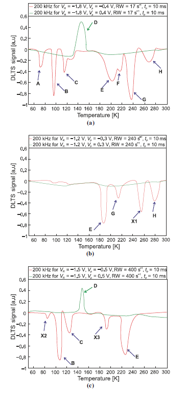
The determined trap parameters (activation energies, Ea and capture cross-sections, σ) are compiled in Table 2. Comparing three steps, traps associated with peaks B, C, and D can lie within the absorber [𝐸𝑔= 177 meV (77 K) and 𝐸𝑔= 240 meV (300 K)]. Peaks B and C can be identi-fied as electron traps (extracted for negative Vp), while peak D can be identified as the hole trap (extracted for positive Vp). The estimated energy levels of peaks B and C are 𝐸c−175 meV and 𝐸c −147 meV, with the corresponding electron capture cross-sections of 8.2 · 10-13 cm2 and 1.2 · 10-16 cm2. The energy level estimated for the peak D is 𝐸v+ 134 meV with a hole capture cross-section of 9.8 · 10-12 cm2. According to the literature, a trap that is characterised by 𝜎= 10-15 − 10-12 cm2, is a typical trap in which the cascade process dominates [1]. Other traps, with 𝜎 = 10-16 − 10-15 cm2 are considered to be neutral [3, 16].
Table 2.
Trap parameters extracted by the DLTS measurements..
Peak |
Step I |
Step II |
Step III |
|||
𝐸𝑎 (meV) |
𝜎 (cm2) |
𝐸𝑎 (meV) |
𝜎 (cm2) |
𝐸𝑎 (meV) |
𝜎 (cm2) |
|
A |
178 |
2.3 ·10−14 |
|
|
|
|
B |
171 |
8.2 ·10-13 |
|
|
179 |
5.3 ·10-13 |
C |
152 |
1.2 ·10−14 |
143 |
7.1 ·10−14 |
||
D |
142 |
9.8 ·10-12 |
125 |
4.4 ·10-12 |
||
E |
189 |
5.7 ·10-15 |
194 |
6.4 ·10-15 |
200 |
8.2 ·10-15 |
F |
300 |
1.7 ·10-16 |
|
|
|
|
G |
353 |
1.2 ·10-16 |
320 |
3.4 ·10-16 |
|
|
H |
380 |
8.2 ·10-16 |
322 |
2.0 ·10−17 |
||
X1 |
|
|
440 |
1.2 ·10-16 |
|
|
X2 |
66 |
2.4 ·10-12 |
||||
X3 |
139 |
7.6 ·10-13 |
||||
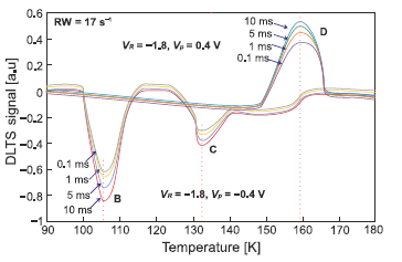
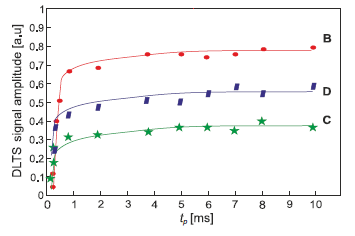
In further analysis, the authors will focus only on peaks lying in the absorber. Fig. 4 presents the DLTS signal extracted for selected values of the filling pulse width 𝑡𝑝, assumed in the range of 0.1-10 ms. The peak positions do not vary with increasing time needed to fill traps and are characterised by exponential carrier capture kinetics (see Fig. 5).
Thus, it can be confirmed that peaks B, C, and D are associated with point defects – most possibly associated with mercury (VHg) and tellurium (VTe) impurity atoms/vacancies occupying cation or anion sites [17, 18]. In As-doped MCT, arsenic impurity can be an acceptor when As atoms take the place of tellurium (AsTe), a donor when arsenic atoms take the place of mercury (AsHg), and a VHg-AsHg complex can also be formed as a slightly deeper acceptor-type level [19].
The defect state energies, concentration and capture cross-sections are summarised in Table 3. Peak B with a trap level of 14 meV concerning the VB edge is a shallow acceptor with the ionization energy consistent with the position of neutral VHg [19, 20]. The determined concen-tration of this trap is 3 · 1014 cm-1. The As dopant may occupy the Hg site and the VHg-AsHg complex is preferably formed due to the existence of VHg. Peak C with a trap level of 42 meV and 1.2 · 1015 cm-1 trap concentration may be linked with the transition related to this complex. Peak D, due to the ionization energy located near CB, is a donor-like defect. It may be related to the single negatively charged VHg state or comes from impurity atoms occupying cation sites. The ionization energy of 132 meV is consistent with the calculated by Kobayashi [15] defect state related to oxygen atoms replacing Hg vacancies. OHg-related defect is created when oxygen atoms accumulated on the sample surface diffuse into the bulk through the Hg vacancies [20]. Since oxygen atoms can only occupy a part of Hg vacancies, a lower concentration of trap D, at a level of 2 · 1013 cm-1, may confirm their origin.
Table 3.
The trap energies and concentration defects for three defects localised in absorber bandgap.
Peak |
T (K) |
Eg (meV) |
Ea (meV) |
ET (meV) |
NT (cm−3) |
𝝈𝝈 (cm2) |
B |
100 |
185 |
EC − 175 |
14 |
3·1014 |
5.3·10-13 |
C |
120 |
190 |
EC − 147 |
42 |
1.2·1015 |
7.1·10−14 |
D |
150 |
198 |
EV + 132 |
132 |
2·1013 |
4.4·10-12 |
Conclusions
The paper shows the method of the DLTS measurements for sophisticated multilayer and low-bandgap devices. Measurements performed for the isolated junctions of the N+/T/p/T/P+/n+ design, allowed the identification of defect states located in the active layer. The presence of three defects level localised within the absorber bandgap was highlighted. One defect can be identified as a hole trap and two as electron ones. Two defects with activation energies of 14 meV and 42 meV create an acceptor-type state, the third one with a trap energy of 132 meV is a deep donor-type defect. All of them are point defect states, most probably stemming from a neutral VHg, VHg-AsHg complex, and OHg-related defect, respectively.
By knowing the origin of the defects, appropriate technological procedures can be taken to reduce their impact on the detector performance. This may be additional post-growth heating or treatments to enhance the physical and chemical stability of the MCT alloy surface.
Authors’ statement
Research concept and design and writing of the article: K.M. Data analysis and interpretation: K.M. and M.K. Critical revision of the article: M.K., K.Mu., and P.M. Final approval of article: K.Mu., M.K., and P.M.
Acknowledgements
This work was financially supported by the National Science Centre (Poland), grant No. UMO-2019/33/B/ST7/ 00614.
References
-
Rogalski, A. HgCdTe infrared detector material: history, status and outlook. Rep. Prog. Phys. 68, 2267 (2005). https://doi.org/10.1088/0034-4885/68/10/R01
-
Lax, M. Cascade capture of electrons in solids. Phys. Rev. 119, 1502–1523 (1960).https://doi.org/10.1103/PhysRev.119.1502
-
Blood, P. & Orton, J. W. The Electrical Characterization of Semi- conductors: Majority Carriers and Electron States. (Academic Press, 1992).
-
Chang, Y. et al. Surface morphology and defect formation mecha- nisms for MCT (211)B grown by molecular beam epitaxy. J. Electron. Mater. 37, 1177–1183 (2008). https://doi.org/10.1007/s11664-008-0477-5
-
Yang, B., Xin, Y., Rujirawat, S., Browning, N. D. & Sivananthan,S. Molecular beam epitaxial growth and structural properties of HgCdTe layers on CdTe (211)B/Si (211) substrates. J. Appl. Phys. 88, 115–119 (2000). https://doi.org/10.1063/1.373631
-
Oda, N., Kanno, T., Saga, M., Oikawa, R. & Maejima, Y. Composition characterization methods for HgCdTe epilayers grown by molecular beam epitaxy. J. Cryst. Growth 117, 193–196 (1992). https://doi.org/10.1016/0022-0248(92)90743-3
-
Zhang, L. H. & Summers, C. A study of void defects in metalorganic molecular-beam epitaxy grown HgCdTe. J. Electron. Mater. 27, 634–639 (1998).https://doi.org/10.1007/S11664-998-0027-1
-
He, L., Fu, X., Wei, Q. & Wang, W. MBE MCT on alternative sub- strates for FPA applications. J. Electron. Mater. 37, 1189–1199 (2008). https://doi.org/10.1007/s11664-008-0441-4
-
Koestner, R. J. & Schaake, H. F. Kinetics of molecular-beam epitaxial HgCdTe growth. J. Vac. Sci. Technol. A 6, 2834–2839 (1988). https://doi.org/10.1116/1.575611
-
Lang, D. V. Deep-level transient spectroscopy: A new method to characterize traps in semiconductors. J. Appl. Phys. 45, 3023–3032 (1974). https://doi.org/10.1063/1.1663719
-
Piotrowski, A. & Kłos, K. Metal-organic chemical vapor deposition of Hg1-xCdxTe fully doped heterostructures without postgrowth anneal for uncooled MWIR and LWIR detectors. J. Electron. Mater. 36, 1052-1058 (2007). https://doi.org/10.1007/s11664-007-0171-z
-
Gawron, W. et al. Recent progress in MOCVD growth for thermoelectrically cooled HgCdTe medium wavelength infrared photodetectors. Solid State Electron. 118, 61–65 (2016). https://doi.org/10.1016/j.sse.2016.01.009
-
Chen, X. D. et al. Deep level defect in Si-implanted GaN n+- pGaN n+-p junction. Appl. Phys. Lett. 82, 3671–3673 (2003). https://doi.org/10.1063/1.1578167
-
Polla, D. L. & Jones, C. E. Deep level studies of Hg1−xCdxTe. I: Narrow-band-gap space-charge spectroscopy. J. Appl. Phys. 52, 5118–5131 (1981).https://doi.org/10.1063/1.329411
-
Kobayashi, A., Sankey, O. F. & Dow, J. D. Chemical trends for defect energy levels in Hg(1-x)CdxTe. Phys. Rev. B 25, 6367 (1982).https://doi.org/10.1103/PhysRevB.25.6367
-
Ciura, L. et al. Investigation of trap levels in HgCdTe IR detectors through low frequency noise spectroscopy. Semicond. Sci. Technol. 31, 035004 (2016). https://doi.org/10.1088/0268-1242/31/3/035004
-
Myles, C. W. Charge state splittings of deep levels in Hg1−xCdxTe. J. Vac. Sci. Technol. A 6, 2675–2680 (1988).
-
Yue, F.-Y. et al. Optical characterization of defects in narrow-gap MCT for infrared detector applications. Chin. Phys. B 28, 017104 (2019).https://doi.org/10.1088/1674-1056/28/1/017104
-
Capper, P. & Garland, J. Mercury Cadmium Telluride Growth, Properties and Applications. (Wiley, UK, 2011).
-
Herman, M. A. & Pessa, M. Hg1−xCdxTe-Hg1−yCdyTe (0≤x, y≤1) heterostructures: Properties, epitaxy, and applications. J. Appl. Phys. 57, 2671–2694 (1985).https://doi.org/10.1063/1.335408