Delay analysis of ring resonator-based beam-forming network in z-domain
- Microwave Photonics Laboratory, Department of Electronics Engineering, Indian Institute of Technology (Indian School of Mines), Dhanbad Jharkhand-826004, India
- Shri Phaneshwar Nath Renu Engineering College, Araria, Bihar 854318, India
Article Info
Received 25 Dec. 2023
Received in revised form 21 Feb. 2024
Accepted 09 Mar. 2024
Available on-line 23 Apr. 2024
Keywords: Antenna element; beam-forming network; optical ring resonator.
Abstract
During the next generation of wireless cellular networks, the millimeter-wave (mm-wave) spectrum will bring new opportunities for exceptionally high data transfer speeds and extensive network connectivity. Millimeter waves, on the other hand, are subject to a significant loss of propagation, which is the most significant impediment. A beneficial solution to this difficulty, which can be overcome, is to use a beam-forming system that consists of many antennas. The purpose of this study is to provide a concept for an integrated photonic beam-forming system that utilises multiple ring resonators for a 1 × 4 phase array antenna operating in the Ka-Band frequency range. The waveguide technology is the foundation for a signal that operates at 28 GHz. It is through the use of the optical ring resonator that the actual time delay line may accomplish its goal. The suggested method can be implemented as a variable true time delay (TTD) line to change the radiation angle of phase array antennas (PAA). The main lobe radiated by the PAA can be directed squint-free between the angles from −28° to +28°. The mathematical analysis and design of the beam producing the structure are presented. Following that, delays of 650 ps, 350 ps, and 250 ps could be produced with coupling coefficients of κ=0.5, κ=0.7, and κ=0.9, respectively, and the associated phase shifts were 0.469π, 0.146π, and 0.387π.
Introduction
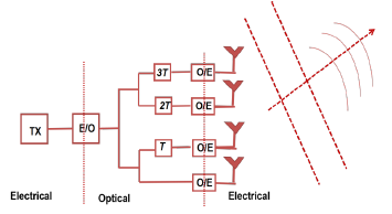
Microwave photonic technology in phase array antennas (PAA) is appealing due to its wide bandwidth operation, antenna remoting, immunity to electromagnetic interference, superior isolation, small size, and low weight [1, 2]. Microwave photonics may perform beam forming, frequency measurement, and signal filtering for phased arrays [3, 4]. Microwave phase shifting is essential for signal conditioning in 5G antenna remote units and military radar systems. Phase shifters require a large radio frequency (RF) range, fast response time, and fine-tuning resolution [5]. Beam forming with many antennas maxi-mizes signal strength in one direction [6]. For high directional gain, many antennas are used in an array to focus the signal on the user, achieving satisfactory efficiency. Conventional electrical beam forming solutions using phase shifters as a delay generator are inefficient and prone to a squinting impact on the beam. For this reason, the system is unable to perform properly at bands with higher frequencies [7, 8] because, as the frequency varies, the beam moves further away from the direction of the target. The network connecting the elements to the transmitter or receiver strongly affects PAA performance. The main job of a beam-forming network (BFN) is to set the right delays to send the signal in the right direction. Beam forming using optical technologies can solve the aforementioned concerns. Many optical beam-forming researchers use the concept of true time delay (TTD). Several optical TTD beam-forming designs have been reported [9, 10]. A simplified form of a TTD-based optical beam-forming system is shown in Fig. 1. For practical considerations in 5G communication networks, smaller devices are required. Realisation of a TTD unit via optical fibre is not sufficient for this purpose. Photonic integration technologies with low attenuation, low weight, tiny size, and independence from frequency can help create a complex beamformer [11].
Switching delay lines [12], photonic crystal fibre [13], and fibre Bragg grating [14] have all been used in the successful realisation of integrated delay line topologies. An optical all-pass ring resonator has a tiny footprint and can constantly tune the delay. In this work, the authors provide a detailed description of an optical ring resonator (ORR)-based 1 × 4 photonic beamformer that uses silicon-on-insulator (SOI) waveguide technology. An mm-wave frequency of 28 GHz is selected because of its low atmospheric effect. Due to its lesser propagation loss and coupling loss with an optical fibre, a SOI rib waveguide is used to construct the photonic beamformer components. One of the guiding layers is made of silicon with a high refractive index (nSi = 3.473 at 1550 nm), and it is bordered by silicon dioxide with a low refractive index (nSiO2 = 1.444). For a TTD line design, the effective refractive index (neff) and group index (ng) of the waveguide must be addressed. Maxwell’s equations were solved using a completely vectorial finite-difference mode solver to get single-mode waveguide dimensions. The effective refractive index and group index, neff and ng at 1550 nm are 2.5 and 5, respectively.
Theory
In Fig. 2, the authors present a schematic layout of the proposed optical beam-forming network (OBFN) for a 1 × 4 linear phased array antenna, an mm-wave signal modulates the laser source continuous light wave in the Mach-Zehnder modulator (MZM), and modulated light from the MZM is connected to a 1 × 4 photonic beam-forming network made up of a 1 × 4 splitter and an all-pass ring resonator. The passive 1 × 4 optical splitter waveguide device splits the modulated light into four different configurations of ring resonators. In the second step, the split signal is sent through a single, double, triple, or quadruple series cascaded ring resonator time delay element to introduce a delay that can be adjusted to achieve a broad range of beam steering. The RF port of MZM receives an RF signal with a frequency of 𝜔𝑅F and amplitude 𝑉𝑒, because of this, the modulated signal with a λ𝑖 carrier wavelength is produced by MZM and can be written as [15]
\( E_{\text {out }(M Z M), i}=\sqrt{P}^j e^{j\left(\omega_i t+\frac{\pi V_e}{V_\pi} \cos \left(\omega_{R F} t\right)\right)} \) (1)
where 𝑉𝜋 is the MZM half-wave voltage and 𝑃𝑖 is the optical power at the corresponding 𝜔𝑖 frequency of the optical carrier signal. The wavelength λ𝑖 of the carrier is linked to the angular frequency 𝜔𝑖. An MZM modulated output is approximated as [16]
\( \begin{aligned} E_{\text {out }(M Z M), i}(t)= & \sqrt{P_i}\left[J_0(\beta) e^{j \omega_i t}+J_1(\beta) e^{j\left(\omega_i t+\omega_{R F} t\right)}\right. \\ & \left.-J_1(\beta) e^{j\left(\omega_i t-\omega_{R F t} t\right.}\right] \end{aligned} \) (2)
MZM modulation index is 𝛽=𝜋𝑉𝑒/𝑉𝜋. Due to the lower value of the phase modulation index, higher-order harmonics are ignored in (2), which yields an equation comparable to the double-sided (DSB)-modulated signal. The electric field at each port of the 1 × 4 splitter is represented as [17]
where 𝑚= 1, 2, 3, 4 (an 𝑛th arm of splitter), 𝐸out,𝑚(𝑡) are the electric fields induced at the output of the 1 × 4 splitter, respectively, 𝛼𝑠 is the waveguide propagation loss in dB/cm. In this work, the waveguide propagation loss 𝛼𝑠 is employed to adjust the ORR to the low-loss scenario. The computed waveguide propagation loss in dB/cm uses the given relation
\( \alpha_s=20 \log \left(e^\alpha\right)=20 \alpha \cdot \log (e)=8.686 \alpha \)
where 𝛼 is the amplitude attenuation constant. The electric field that is produced at the output of the beamformer is then transmitted to the photodiode (PD) after it has been transmitted through a waveguide with a length of 𝐿𝑤. The electric field induced at each PD is given by
\( E_{P D m_{\text {in }}}(t)=E_{\text {out }, m}(t)\left(-j \beta L_w\right) \exp \left(\frac{-\alpha L_w}{2}\right) H_p(f) \) (4)
where 𝐻𝑝(𝑓) is the transfer function of the different configurations of ring resonators and 𝑝𝑝 is the number of rings connected in a cascaded form. Similarly, the induced electric field of the beamformer through ring and waveguide is fed to the photodiodes (PDs) PD1, PD2, PD3, PD4 after propagating through a different configuration of a cascaded ring resonator of each port of the PDs which are given by below relation
\( \begin{aligned} & E_{P D m_{\text {in }}}(t) \\ & =E_{\text {out }, m}(t)\left(-j \beta L_{w m}\right) \exp \left(\frac{-\alpha L_{w m}}{2}\right) H_p(f) \\ & =\frac{E_{\text {out }(M Z M), i} 10^{\frac{-\alpha_s}{20}}}{2}\left(-j \beta L_{w m}\right) \exp \left(\frac{-\alpha L_{w m}}{2}\right) H_p(f) \end{aligned} \) (5)
Substituting 𝐸out,𝑚(𝑡) value in (5), the authors obtain:
\( \begin{aligned} &\begin{aligned} & E_{P D m_{\text {th }}}(t) \\ & =\frac{\sqrt{P_i}\left[J_0(\beta) e^{j \omega_l t}+J_1(\beta) e^{j\left(\omega_i t+\omega_{R P t} t\right)}-J_1(\beta) e^{j\left(\omega_i t-\omega_{R P} t\right)}\right] 10^{\frac{-\alpha_s}{20}}}{2} \\ & \cdot\left(-j \beta L_{w m}\right) \exp \left(\frac{-\alpha L_{w m}}{2}\right) H_p(f) \end{aligned}\\ \end{aligned} \) (6)
where 𝐻𝑝(𝑓) are the transfer functions of different configurations of the ring with rectangular waveguides and 𝐿𝑤m is the corresponding length of the waveguide.
The signal from the beam-forming network is fed to PD1, PD2, PD3, and PD4 to provide an RF signal of different power. Table 1 shows modelling with derivation of a single and series multiple cascaded ring resonator using Mason’s gain rule. These cascading structures are working as a beam-forming network. PD output provides a photonic RF signal, which has different magnitudes and phases or delays which will ensure the antenna excitation and radiation pattern in the far field. This magnitude and phases depend on the transfer function of the ring resonator or series cascaded ring resonators. And the transmittance of the given structure mainly depends on phase (𝜑) and coupling coefficient (κ), the photocurrent in the PDs is represented as
\( I_{P D m_{\text {out }}}(t)=R_{P D}\left|E_{P D m_{\text {in }}}(t)\right|^2+I_{P D m_N}(t) \) (7)

where 𝐼PDmout(𝑡) is the photocurrent as measured at the corresponding PD output, RPD is the responsivity of PDs. 𝐼PDmN(𝑡) reflects the contribution to the noise current made by several different causes, including shot noise and dark current noise in PDs so the equation of PD current at the output of PD is
\( \begin{aligned} & I_{P D m_{\text {out }}}(t) \\ & =R_{P D}\left|\frac{\sqrt{P_i}\left[J_0(\beta) e^{j \omega_i t}+J_1(\beta) e^{j\left(\omega_i t+\omega_{R P} t\right)}-J_1(\beta) e^{j\left(\omega_i t-\omega_{R P t} t\right.}\right] 10^{-\alpha_S / 20}}{2}\left(-j \beta L_{w m}\right) \exp \left(\frac{-\alpha L_{w m}}{2}\right) H_p(f)\right|^2+I_{P D m_N}(t) \end{aligned} \) (8)
It is clear from the aforementioned equations that the photocurrent at the PD output is affected by several factors, including the coupling coefficient, waveguide loss, round-trip path length, and phase shift of the all-pass ring resonator.
As per the proposed beam-forming system as shown in Fig. 2, the incoming signal will be linked into the first ring at the MZM output with a coupling coefficient of κ, as the remaining very less amount of signal propagates through the straight waveguide to the through-port that is not sufficient to excite the PD. With the same coupling coefficient κ, the portion of the signal that travels in the ring will be linked once again into the waveguide beneath the ring. These phenomena provide some delay signal concerning the reception without a ring at the PD output. For all the rings, this propagation operation continues. There will be a series cascaded combination of one, two, three, and four rings that will interact with the straight waveguides bus of each unit. The rings that are at the top and bottom of the cascade will be the rings that interact with the waveguides bus that leads to the through-port and drop-port, respectively. The interaction between the rings in this configuration is direct and takes the form of propagation between rings themselves. All tests will be conducted with a coupling coefficient of 0.5, 0.7, and 0.9 and ring lengths are 14.42 μm, 16.48 μm, 19.57 μm, and 29 μm. Effective refractive index neff = 2.5, group index ng = 5 simulating the effects of cascading exclusively.

Modelling of ring resonator for time delay analysis in z-domain
Light is an electromagnetic wave, but it is a time variable, as well as a space variable. Moslehi [18] has experimentally shown that when light waves travel through a waveguide, then their delay can be represented as a conventional transfer function of delay. The transfer function of delay can be represented in the Laplace domain, as well as the z-domain. The most fundamental element useful to represent Bragg grating could be a partially reflected mirror which is equivalent to the well-known Fabry-Perot (FP) cavity. In a typical all-pass configuration, as shown in Fig. 3(a), the Z-transform schematic of the single ring resonator is represented in Fig. 3(b), a straight waveguide is positioned next to a ring near a couple that allows light to pass in and out of the resonator via an evanescent field.

The input complex mode amplitude, Ei , and the output complex mode amplitude, 𝐸t, are the normalised measurements of the complex modes in the straight waveguide. Both t and κ represent waveguide fields through the coupling coefficient and the cross-over coupling coefficient, respectively. Such that 𝑡2+κ2=1. The interaction between light and the attenuation constant in the ring resonator filter is shown in Fig. 3(b) and can be characterised by the matrix relation as in (9). Here, it can be considered 𝐶1=𝐶2=𝐶 and 𝑆1=𝑆2=𝑆..
\( \left[\begin{array}{l} E_{t 1} \\ E_{t 2} \end{array}\right]=a\left[\begin{array}{cc} C & j S \\ -j S^* & C^* \end{array}\right]\left[\begin{array}{l} E_{i 1} \\ E_{i 2} \end{array}\right] \) (9)
Coupler inputs are denoted by 𝐸𝑖 1 and 𝐸𝑖 2 whereas coupler outputs are denoted by 𝐸t1 and 𝐸t2, and the amplitude transmission coefficient of the coupler is denoted by a. The representation of the through-port transmission is denoted by the equation 𝐶=√1−κ, while the designation of the cross-port transmission would be −𝑗S =−𝑗√κ, the coupling ratio κ should be wavelength-independent; the effective group index is constant and does not vary from its nominal value. The transfer function of a ring resonator can be calculated using the Mason’s gain formula [19, 20]. The ring round-trip loss can be expressed as 𝛼𝑠 = exp(𝛼L) [21], where 𝛼 is the average ring loss per unit length and L is the circumference of the ring. One is chosen as the amplitude transmission coefficient. The total transmittance of a single ring with a single waveguide is defined as
\( H(f)=\frac{S_1 S_2 \sqrt{\alpha_s z^{-1}}}{1-C_1 C_2 \alpha_s z^{-1}} \) (10)
where 𝑧−1 is generally known as the unit delay in the z-domain and the entire ring perimeter represents the unit delay length for a single ring resonator; 𝑧−1=𝑒−(𝛼+𝑗ß)𝐿 and assuming the loss is not considered here; 𝛼 is the amplitude attenuation constant and 𝛽 is the propagation constant given by 𝛽=2𝜋neff/𝜆 ; 𝐿 is the circumference of the resonator. Assuming that there is no propagation loss in the resonator, i.e., all power coming to the input port reaches the output port. Then 𝛼 will be zero and the magnitude of the transfer function will be 1. Similarly, Table 1 shows the structural representation and transmittance with derivation using Mason’s gain rule of the single, double, triple, and quad-ring resonator. The idea of group delay is used to demonstrate the delay characteristics of the ORR. The transfer function 𝐻(𝑓) of any signal using signal flow graph (SFG) as per the Meson’s gain rule is given by
\( H(f)=\frac{\sum T_n \Delta_n}{\Delta} \) (11)
In the above equation, 𝑇𝑛 represents the transmittance of the nth forward path, and Δ represents the determinant of the graph
\( \Delta=1-\sum L_1+\sum L_2+\sum L_3+\cdots \)
In this context, Σ𝐿1 denotes the total transmittance of all specific graphs of single closed paths (loops), Σ𝐿2 denotes the total transmittance of all potential permutations of two non-touching closed paths, Σ𝐿3 denotes the total transmittance of all potential permutations of three non-touching loops, and so on. It is important to note that Δn represents the value of Δ for the portion of the graph that does not touch the 𝑛th forward path. Table 1 presented below delineates the derivation of transfer functions for single, double, triple, and quad-ring resonators in tabular format. Phase of 𝐻(𝑓) is
\( \emptyset=\tan ^{-1}\left(\frac{\operatorname{Re}\{H(f)\}}{\operatorname{Im}\{H(f)\}}\right) \)
and group delay is defined as [22]
\( \tau_{G D}(f)=-\frac{d \emptyset}{d \omega} \) (12)
After simplification, the frequency-dependent group delay of one ring and one waveguide can be expressed using the following mathematical expression
\( \tau_{G D}(f)=\frac{\kappa \tau_r}{\left(2-\kappa-2 \sqrt{1-\kappa} \cos \left(2 \pi f \tau_r+\varphi\right)\right)} \) (13)
where 𝜏𝑟=𝑛 𝑒ff𝐿/𝑐. Fig. 4 and 5 show the transmittance spectrum and group delay spectrum of single, double, triple, and quad-ring resonator configuration, respectively, The derivation of all four structures of cascaded ring resonator are discuss in Table 1.


From the transmittance graph, the free spectral range (FSR) value for finding the delay generated by each configuration of the ring resonator can be calculated. As in (8), it is clear that the coupling coefficients of the all-pass ring resonator affect the photocurrent at the PD output. In Fig. 6, the group delay plot shows the variation of coupling coefficient for three different values, at κ= 0.5, κ= 0.7, and κ= 0.9, respectively. When an ORR is used as an optical delay element, this feature is the most important one. For the proposed ORR to meet the low-loss condition, it is assumed that the round-trip loss 𝛼s is less than 1 dB. The frequency response of an ORR is controlled by the coupling ratio and the additional round-trip phase shift, which determine the offset of the resonance frequency. When κ = 0, nothing at all of the incoming light connects to the ring, the ORR produces no phase shifts or delays. In the case when κ equals 1, the light that is introduced connects entirely to the ring, and then completely disconnects after a single round-trip. In this particular scenario, the ORR performs the same function as a waveguide with dimensions of 2 × 2, so the coupling coefficient κ should lie in the range of 0<κ<1.
After one FSR, the phase transition is 2𝜋. However, if the value of κ is lower than the critical coupling point, a negative group delay will occur in the area of the resonance frequency for a lossy ORR [23]. From Fig. 6, the coupling of coefficient of κ= 0.5, κ= 0.7, and κ= 0.9 is taken to find the group delay response. By selecting the appropriate phase 𝜑 and the coupling coefficient κ of every individual ORR in the in-series cascaded structure, a smooth delay band with a wide bandwidth will be obtained as shown in Fig. 7. It is evident that the delay band formed a ripple and is not perfectly smooth; the ripple will cause different frequency components of the signals that fall within the delay band to experience unequal delays as a result. These ripples cause changes in the antenna beam angle when ORRs are used in an OBFN as the delay elements [24, 25].


Beam-forming system based on multiple ORR structures
By introducing the round-trip phase shift 𝜑 of the ring resonator, the group delay response in (12) is derived by putting 𝜏𝑟=𝑛𝑔𝐿/𝑐 as the round-trip propagation time where the speed of light is denoted by the letter 𝑐𝑐. The group delay responses for beam-forming network using coupling coefficients of κ=0.5, κ=0.7, and κ=0.9 in the ring resonator for single, double, triple, and quadruple structures are shown in Fig. 8. The simulated and theoretical group delay achieved between the waveguides of the TTD lines of the proposed beam-forming system are shown in Table 2, respectively. Thus, the time delay achieved by the proposed beam-forming system for κ=0.5, κ=0.7, and κ=0.9 Δ𝜏0= 650 ps, Δ𝜏0= 350 ps, and Δ𝜏0= 250 ps.

According to the theory of true-time delay-based beam-forming system, the relation between the expected beam angle 𝜃0 and the necessary inter-element phase difference Δ∅0 is as follows:
\( \Delta \emptyset_0=k d \sin \theta_0 \) (14)
where 𝑘= 2𝜋/λRF, λsRF is the wavelength of a signal in free space denoted by λRF, and the distance between antenna elements is denoted by d. Using the formula provided, with a constant inter-element spacing linear array antenna, the desired beam angle in the far-field radiation pattern can be generated by defining the incremental time delay that must be maintained between adjacent waveguides of an optical TTD unit. This will allow the antenna to produce the desired beam angle
\( \Delta \tau_0=\frac{k d \sin \theta_0}{2 \pi f_{R F}} \) (15)
To prevent the formation of grating lobes, it is recommended that the spacing d between adjacent elements be equal to λRF/2. After making the substitutions k = 2𝜋/λRF and λRF/2, the above equation becomes
\( \Delta \tau_0=\frac{\sin \theta_0}{2 f_{R F}} \) (16)
\( \theta_0=\sin ^{-1}\left(2 f_{R F} \Delta \tau_0\right) \) (17)
based on the incremental time delay Δ𝜏𝜏0 transmission of the signal. Equation (17) demonstrates that the antenna radiates in a particular direction 𝜃0.
Simulated results and analysis for beam-forming steering
In this study, the authors use the idea of a group delay to describe the properties of the delay that the modulated RF signal encounters. The group delay is defined as the inverse of the phase response of the transfer function in an ORR as a function of the angular frequency ω. Here, there is a formula for a group delay that takes into account the frequency component [26, 27]
\( \tau_{G D}=-\frac{d \varphi(\omega)}{d \omega} \) (18)
The frequency-dependent incremental group delay can be expressed in (18). Table 2 shows the theoretical and achievable different delays for the different cascaded structures of the beam-forming system. Fig. 9 shows the polar plot of the beam-forming radiation pattern of different frequencies from 28–34 GHz. From Table 2, the authors found that the theoretical value of the beam angle has a good resemblance with the simulation one, in some cases, both theoretical and simulated results overlapped and could not be distinguish in these plots.

Table 2.
Group delay response of all cascaded configurations of the ring resonator.
Operative frequency 𝒇RF |
Delay (ps) 𝝉GD |
Delay (ps) ∆𝝉𝟎 = 𝝉GD − 𝝉GDn−𝟏 |
Beam angle (theoretical) 𝜽𝟎 = 𝐬in(𝒇𝑹F∆𝝉𝟎) |
Beam angle (simulated) |
28 GHz |
250 |
250 |
8.0° |
7.65° |
30 GHz |
500 |
250 |
8.62° |
8.16° |
32 GHz |
750 |
250 |
9.20° |
9.07° |
34 GHz |
1000 |
250 |
9.78° |
9.56° |
Table 1 has been followed to obtain Fig. 9, which shows the actual beam-forming response in the polar plot of each unit of the beam-forming network at a frequency of 28–34 GHz. Delay of the proposed different cascaded architecture of ring resonator as a delay element which corresponds to a beam directing angle of −28°, +28°, 0° for coupling coefficient of κ=0.5, κ=0.7, and κ=0.9, respectively.

Tables 3, 4, and 5 show the theoretical and simulated beam angle for different coupling coefficients at 28 GHz. Fig. 10 depicts beam-forming angles at 28 GHz of −28°, +28°, and 0° for the coupling coefficient of κ=0.5, κ=0.7, and κ=0.9, respectively. According to the literature, as the number of antennas remains constant, the back-lobe power increases as the scan angle grows larger. Power is emitted in an unacceptable direction. More antennas can be employed to suppress back lobes and boost main lobe output. This study uses a group delay to illustrate the modulated RF signal temporal delay. Fig. 11 demonstrates the relationship between steering angle and time delay for different mm-wave frequencies. A 250 ps delay was achieved between the TTD lines of the beamformer using a single, double, triple, and quadruple cascaded structure of ring resonator. The phase difference value was 0.387π, and the steering angle ranged from −28° to +28° at an mm-wave frequency of 28 GHz.

Table 3.
Theoretical and simulated beam angle for coupling coefficient of κ=0.5 at 28GHz
Operative frequency 𝒇RF(GHz) |
Coupling coefficient (k) |
Delay element structure |
Group delay (ps) 𝝉GD |
Delay (ps) ∆𝝉𝟎 = 𝝉GDn− 𝝉GDn-1 |
Beam angle (theoretical) 𝜽𝟎 = 𝐬in(𝒇RF∆𝝉𝟎) |
Beam angle (simulated) |
|
|
Single ring |
650 |
|
|
|
|
|
Double ring |
1300 |
|
|
|
28 |
0.5 |
Triple ring |
1950 |
650 |
+28.0° |
+26.65° |
|
|
Quad ring |
2600 |
|
|
|
Table 4.
Theoretical and simulated beam angle for coupling coefficient of κ=0.7 at 28 GHz
Operative frequency 𝒇RF(GHz) |
Coupling coefficient (k) |
Delay element structure |
Group delay (ps) 𝝉GD |
Delay (ps) ∆𝝉𝟎 = 𝝉GDn− 𝝉GDn-1 |
Beam angle (theoretical) 𝜽𝟎 = 𝐬in(𝒇RF∆𝝉𝟎) |
Beam angle (simulated) |
|
|
Single ring |
350 |
|
|
|
|
|
Double ring |
700 |
|
|
|
28 |
0.7 |
Triple ring |
1050 |
350 |
0° |
0.25° |
|
|
Quad ring |
1450 |
|
|
|
Table 5.
Theoretical and simulated beam angle for coupling coefficient of κ=0.9 at 28 GHz.
Operative frequency 𝒇RF (GHz) |
Coupling coefficient (k) |
Delay element structure |
Group delay (ps) 𝝉GD |
Delay (ps) ∆𝝉𝟎 = 𝝉GDn− 𝝉GDn-1 |
Beam angle (theoretical) 𝜽𝟎 = 𝐬in(𝒇RF∆𝝉𝟎) |
Beam angle (simulated) |
|
|
Single ring |
250 |
|
|
|
|
|
Double ring |
500 |
|
|
|
28 |
0.9 |
Triple ring |
750 |
250 |
−28.0° |
−26.65° |
|
|
Quad ring |
1000 |
|
|
|
Conclusions
In this paper, the authors present a proposal for a ring resonator-based photonic beam-forming network for 28–34 GHz transmissions, i.e., based on waveguide technology. It is necessary to make use of the micro-ring resonator to successfully construct the actual time delay line. The design of ring resonators with radiI of 14.42 μm, 16.48 μm, 19.57 μm, and 29 μm, respectively, is currently being computed using waveguide technology. The next step is to outline the beam-forming structure design, after which the mathematical analysis will be presented. The group delay might be set to 650 ps, 350 ps, or 250 ps for coupling coefficient of κ=0.5, κ=0.7, and κ=0.9, respectively, and corresponding phase shifts are 0.469𝜋, 0.146𝜋 , 0.387𝜋, respectively.
Acknowledgements
This work is carried out from the research grant under the grant no.: ERIP/ER/202206004/M/01/1805 (Sanction Code of ER&IPR: DGTM/ERIP/GIA/22-23/115/008 dated 08/08/2022) provided by Defence Research and Development Organization (DRDO), Government of India (GOI) under Extramural Research funding scheme with the project entitled “Design and Development of Frequency Stable and High Q-Factor Optoelectronic Oscillator Assisted by Microwave Photonic Techniques”.
References
-
Minasian, R. A. Ultra-wideband and adaptive photonic signal processing of microwave signals. IEEE J. Quantum Electron. 52, 1– 13 (2016). https://doi.org/10.1109/JQE.2015.2499729
-
Minasian, R. A., Chan, E. H. W. & Yi, X. Microwave photonic signal processing. Opt. Express 21, 22918–22936 (2013). https://doi.org/10.1364/OE.21.022918
-
Yi, X., Chew, S. X., Song, S., Nguyen, L. & Minasian, R. A. Integrated microwave photonics for wideband signal processing.Photonics 4, 46 (2017). https://doi.org/10.3390/photonics4040046
-
Minasian, R. A. Photonic signal processing of microwave signals. IEEE Trans. Microw. Theory Tech. 54, 832–846 (2006). https://doi.org/10.1109/TMTT.2005.863060
-
Nguyen, T. A., Chan, E. H. W. & Minasian, R. A. Instantaneous high-resolution multiple-frequency measurement system based on frequency-to-time mapping technique. Opt. Lett. 39, 2419–2422 (2014). https://doi.org/10.1364/OL39002419
-
Sadhu, B. et al. A 28 GHz 32-Element Phased-Array Transceiver IC with Concurrent Dual Polarized Beams and 1.4 Degree Beam- Steering Resolution for 5G Communication. in 2017 IEEE International Solid-State Circuits Conference (ISSCC) 3373–3391 (IEEE, 2017). https://doi.org/10.1109/JSSC.2017.2766211
-
Nadeem, M. D. & Raghuwanshi, S. K. Optimised design & analysis of high gain 3×3 square patch array antennas with six ports for airborne application in S-band. J. Electromagn. Waves Appl. 36, 2419–2434 (2022). https://doi.org/10.1080/09205071.2022.2080592
-
Aluigi, L., Orecchini, G. & Larcher, L. A 28 GHz Scalable Beamforming System for 5G Automotive Connectivity: An Integrated Patch Antenna and Power Amplifier Solution. in 2018 IEEE MTT-S International Microwave Workshop Series on 5G Hardware and System Technologies (IMWS-5G) 1–3 (IEEE, 2018). https://doi.org/10.1109/IMWS-5G.2018.8484325
-
Akiyama, T., Ando, T. & Hirano, Y. Fourier Transform Optically Controlled Phased Array Antenna. in 2013 18th OptoElectronics and Communications Conference held jointly with 2013 International Conference on Photonics in Switching WO4_4 (OSA, 2013). https://doi.org/10.1364/OECC_PS.2013.WO4_4
-
Ortega, B., Mora, J. & Chulia, R. Optical beamformer for 2-D phased array antenna with subarray partitioning capability. IEEE Photon. J. 8, 1–9 (2016). https://doi.org/10.1109/JPHOT.2016.2550323
-
Li, Y., Ghafoor, S., Satyanarayana, K., El-Hajjar, M. & Hanzo, L. Analogue wireless beamforming exploiting the fiber-nonlinearity of radio over fiber-based C- RANs. IEEE Trans. Veh. Technol. 68, 2802–2813 (2019). https://doi.org/10.1109/TVT.2019.2893589
-
Jung, B. M. & Yao, J. A two-dimensional optical true time-delay beamformer consisting of a fiber Bragg grating prism and switch- based fiber-optic delay lines. IEEE Photon. Technol. Lett. 21, 627– 629 (2009). https://doi.org/10.1109/LPT.2009.2015275
-
Sancho, J. et al. Integrable microwave filter based on a photonic crystal delay line. Nat. Commun. 3, 1075 (2012). https://doi.org/10.1038/ncomms2092
-
Kumar, S. N. & Raghuwanshi, S. K. Demonstration of Highly Steerable Beamforming System Incorporating a Waveguide of Spatially Distributed Fiber Bragg Grating. in 2019 6th International Conference on Signal Processing and Integrated Networks (SPIN) 367–370 (IEEE, 2019). https://doi.org/10.1109/SPIN.2019.8711766
-
Kumar, R., Raghuwanshi, S. K. & Nadeem, D. Chirped fiber grating and specialty fiber based multiwavelength optical beamforming network for 1X8 phased array antenna in S-band. Optik 243, 167044 (2021). https://doi.org/10.1016/j.ijleo.2021.167044
-
Kumar, R. & Raghuwanshi, S. K. photonic generation of multiple shapes and sextupled microwave signal based on polarization modulator. IEEE Trans. Microw. Theory Tech. 69, 3875–3882 (2021). https://doi.org/10.1109/TMTT.2021.3076996
-
Kumari, S. &, Prince, S. Photonic beamforming incorporating ring resonator based on silicon-on-insulator waveguide technology. Silicon 14, 8869–8879 (2022). https://doi.org/10.1007/s12633-022-01684-w
-
Moslehi, B., Goodman, J. W., Tur, M. & Shaw, H. J. Fiber-optic lattice signal processing. Proc. IEEE 72, 909–930 (1984). https://doi.org/10.1109/PROC.1984.12948
-
Rabus, D. G. Ring Resonators: Theory and Modeling. Integrated Ring Resonators. (Springer Berlin Heidelberg, 2007).
-
Kumar, R., Singh, Y., Raghuwanshi, S. K., Chandra, S. & Nadeem, D. Delay and Dispersion Investigation of Optical Components for, Microwave Photonic Filter. in ,VLSI, Microwave and Wireless Technologies. Lecture Notes in Electrical Engineering (eds. Mishra, B. & Tiwari, M.) vol. 877 (Springer, 2023). https://doi.org/10.1007/978-981-19-0312-0_69
-
Kumari, S. & Prince, S. Photonic integrated cmos-compatible true time delay based broadband beamformer. Opt. Quant. Electron. 55, 1198 (2023). https://doi.org/10.1007/s11082-023-05492-3
-
Roeloffzen, C. G. H. et al. Integrated photonic beamformer employing continuously tunable ring resonator-based delays in CMOS- compatible LPCVD waveguide technology. Proc. SPIE 7135, 71341K (2008). https://doi.org/10.1117/12.803719
-
Nadeem, D. et al. Design and analysis of photonic beam forming system using ring resonator for 1 × 4 phase array antenna in Ka- Band. Proc. SPIE 12429, 124290S (2023). https://doi.org/10.1117/12.2648280
-
Nadeem, D. et al. Modeling of quad ring resonator for tunable delay line in z-domain analysis. Proc. SPIE 12429, 114290N (2023). https://doi.org/10.1117/12.2648319
-
Nadeem, M. D., Raghuwanshi, S. K. & Kumar, R. Efficient photonics beam forming system incorporating super structure fiber Bragg grating for application in Ku band. Opt. Fiber Technol. 80, 103436 (2023). https://doi.org/10.1016/j.yofte.2023.103436
-
Nadeem, D., Kumar, R., Raghuwanshi, S. K. & Kumar, S. Advanced photonic-assisted antenna array: efficient beam steering system for radar application. Proc. SPIE 12890, 128900J-1 (2024). https://doi.org/10.1117/12.2691273
-
Danish, N., Sanjeev, K. R. & Yadav, R. K. Recent advancement on photonic feeding antennas for microwave beam steering. I- Manager’s J. Commun. Eng. Systems (JCS) 8, 10 (2019). https://doi.org/10.26634/jcs.8.1.15888